Quantum lithography surpasses traditional electron beam lithography by utilizing quantum entanglement to achieve higher resolution patterns beyond the diffraction limit, enabling more precise nanoscale fabrication. Explore the article to understand how your choice between these cutting-edge techniques can impact the future of semiconductor manufacturing.
Table of Comparison
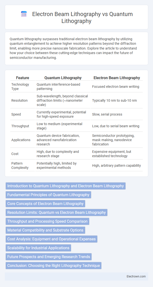
| Feature | Quantum Lithography | Electron Beam Lithography |
|---|---|---|
| Technology Type | Quantum interference-based patterning | Focused electron beam writing |
| Resolution | Sub-wavelength, beyond classical diffraction limits (~nanometer scale) | Typically 10 nm to sub-10 nm |
| Speed | Currently experimental, potential for high-speed exposure | Slow, serial process |
| Throughput | Low to medium (experimental stage) | Low, due to serial beam writing |
| Applications | Quantum device fabrication, advanced nanofabrication research | Semiconductor prototyping, mask making, nanodevice fabrication |
| Cost | High, due to complexity and research stage | Expensive equipment, but established technology |
| Pattern Complexity | Potentially high, limited by experimental methods | High, arbitrary pattern capability |
Introduction to Quantum Lithography and Electron Beam Lithography
Quantum lithography leverages quantum entanglement and interference to achieve patterning beyond the classical diffraction limit, offering potential for ultra-high resolution in nanofabrication. Electron beam lithography (EBL) uses a focused beam of electrons to directly write intricate patterns on a resist-coated substrate, widely favored for precise and flexible manufacturing at the nanoscale. Understanding these advanced lithography techniques allows you to explore cutting-edge methods for creating next-generation semiconductor devices with enhanced resolution and accuracy.
Fundamental Principles of Quantum Lithography
Quantum lithography leverages the principles of quantum entanglement to surpass classical diffraction limits, enabling patterning at scales smaller than the wavelength of light. Unlike electron beam lithography, which uses focused electron beams to etch materials with high precision, quantum lithography exploits non-classical light states to achieve ultra-high resolution through interference effects. Your ability to fabricate nanoscale features benefits from the fundamentally different approach of quantum lithography, which promises enhanced spatial resolution beyond traditional electron-based methods.
Core Concepts of Electron Beam Lithography
Electron beam lithography (EBL) utilizes a focused beam of electrons to directly write patterns on a resist-coated substrate, enabling nanometer-scale resolution beyond optical limits. The core concept relies on the electron scattering interactions with the resist material, which alters its solubility to create precise features. EBL offers high patterning flexibility and resolution but generally has slower throughput compared to traditional lithography methods like quantum lithography.
Resolution Limits: Quantum vs Electron Beam Lithography
Quantum lithography leverages quantum entanglement and interference to potentially surpass classical diffraction limits, achieving resolutions beyond the capabilities of electron beam lithography (EBL). Electron beam lithography, while offering high precision down to approximately 10 nanometers, is constrained by electron scattering and resist sensitivity, limiting further miniaturization. Your choice between these techniques depends on the trade-off between current technological maturity of EBL and the emerging potential quantum lithography holds for ultra-high resolution patterning in nanofabrication.
Throughput and Processing Speed Comparison
Quantum lithography offers the potential for higher throughput by utilizing quantum interference patterns to write features below the diffraction limit faster than conventional electron beam lithography (EBL), which relies on serial electron spot scanning and inherently slower processing speeds. EBL provides high resolution but suffers from limited throughput due to its serial nature, making it less suitable for large-scale manufacturing compared to the parallel processing advantage quantum lithography might achieve. Your choice between the two depends on whether speed and volume (throughput) or proven precision and established technology are the priority for your nanofabrication needs.
Material Compatibility and Substrate Options
Quantum lithography enables patterning on a wider range of materials, including delicate polymers and biological substrates, due to its low-energy photon interactions. Electron beam lithography (EBL) is highly effective on traditional semiconductor materials like silicon and gallium arsenide but can cause substrate damage or charging issues on insulating or fragile materials. Quantum lithography also offers better compatibility with flexible and thin-film substrates, expanding possibilities for next-generation electronics and photonics fabrication.
Cost Analysis: Equipment and Operational Expenses
Quantum lithography demands cutting-edge laser systems and advanced quantum light sources, resulting in higher initial equipment costs compared to electron beam lithography (EBL). EBL involves significant expenses related to electron beam generators, vacuum systems, and beam control electronics, but benefits from established manufacturing and maintenance infrastructure that can reduce operational costs. Operationally, quantum lithography may incur increased costs due to complex quantum state preparation and lower throughput, whereas EBL's slower patterning speeds raise labor and time expenses despite more mature technology.
Scalability for Industrial Applications
Quantum lithography promises ultra-high resolution beyond the diffraction limit, but its practical scalability for industrial applications remains constrained by complex setups and delicate quantum states. Electron beam lithography (EBL) offers established scalability with precise patterning at the nanoscale, supported by mature manufacturing infrastructure and automation. Industrial adoption heavily favors EBL due to reliable throughput and integration with existing semiconductor fabrication processes, whereas quantum lithography is still in experimental stages with limited scalability for mass production.
Future Prospects and Emerging Research Trends
Quantum lithography leverages entangled photons to achieve resolution beyond the diffraction limit, promising significant advancements in nanofabrication and semiconductor manufacturing. Emerging research trends emphasize integrating quantum lithography with conventional electron beam lithography (EBL) to overcome EBL's limitations in throughput and feature size, aiming for scalable, ultra-high-resolution patterning. Future prospects include the development of hybrid quantum-electron beam systems and improved photon source stability, which could revolutionize the production of next-generation quantum devices and nanoscale circuits.
Conclusion: Choosing the Right Lithography Technique
Quantum lithography offers the potential for ultra-high resolution beyond the diffraction limit using entangled photons, making it ideal for next-generation nanofabrication. Electron beam lithography provides established, precise patterning with sub-10 nm resolution and versatility for a wide range of materials, suited for current semiconductor manufacturing and research. Selecting the right lithography technique depends on balancing resolution needs, fabrication speed, cost constraints, and technological maturity.
quantum lithography vs electron beam lithography Infographic