Photonic bandgap refers to a range of frequencies in which light cannot propagate through a material, while electronic bandgap pertains to the energy range where electrons are forbidden in a solid, crucial for semiconductors. Understanding these differences can enhance your grasp of material properties and their applications in technology; explore the full article for deeper insights.
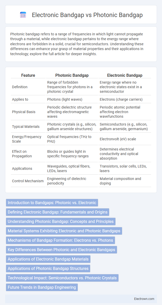
Table of Comparison
| Feature | Photonic Bandgap | Electronic Bandgap |
|---|---|---|
| Definition | Range of forbidden frequencies for photons in a photonic crystal | Energy range where no electronic states exist in a semiconductor |
| Applies to | Photons (light waves) | Electrons (charge carriers) |
| Physical Basis | Periodic dielectric structure affecting electromagnetic waves | Periodic atomic potential affecting electron wavefunctions |
| Typical Materials | Photonic crystals (e.g., silicon, gallium arsenide structures) | Semiconductors (e.g., silicon, gallium arsenide, germanium) |
| Energy/Frequency Scale | Optical frequencies (THz to PHz) | Electronvolt (eV) scale |
| Effect on Propagation | Blocks or guides light in specific frequency ranges | Determines electrical conductivity and optical absorption |
| Applications | Waveguides, optical fibers, LEDs, lasers | Transistors, solar cells, LEDs, lasers |
| Control Mechanism | Engineering of dielectric periodicity | Material composition and doping |
Introduction to Bandgaps: Photonic vs. Electronic
Photonic bandgaps refer to the range of light frequencies that cannot propagate through a photonic crystal due to its periodic dielectric structure, analogous to how electronic bandgaps represent energy ranges in semiconductors where electron states are forbidden within the material's periodic atomic lattice. Electronic bandgaps determine electrical conductivity and semiconducting behavior by inhibiting electron flow at certain energy levels, whereas photonic bandgaps control the flow of electromagnetic waves and enable manipulation of light propagation in optical devices. Understanding the distinction between photonic and electronic bandgaps is critical in fields like optoelectronics, photonic crystal design, and semiconductor physics for tailoring material properties to specific applications.
Defining Electronic Bandgap: Fundamentals and Origins
The electronic bandgap represents the energy difference between the valence band and the conduction band in a semiconductor or insulator, determining the material's ability to conduct electricity. It originates from the quantum mechanical interactions of electrons within the atomic lattice, resulting in allowed and forbidden energy states. This intrinsic property defines a material's electrical conductivity and optical absorption characteristics, crucial for electronic and optoelectronic device performance.
Understanding Photonic Bandgap: Concepts and Principles
Photonic bandgap refers to a range of frequencies within which electromagnetic waves cannot propagate through a photonic crystal, analogous to the electronic bandgap where electronic states are forbidden in a semiconductor. The concept relies on periodic dielectric structures that create interference patterns blocking specific wavelength ranges, controlling light propagation with precision. Understanding photonic bandgap principles enables innovations in optical devices, such as waveguides and filters, by manipulating light in ways that traditional electronic bandgaps control electron flow.
Material Systems Exhibiting Electronic and Photonic Bandgaps
Semiconductor materials such as silicon and gallium arsenide exhibit electronic bandgaps critical for controlling electron flow in electronic devices. Photonic bandgap materials include photonic crystals made from dielectric materials like silicon dioxide or titanium dioxide, which manipulate light propagation through periodic refractive index variations. Both material systems rely on periodic structures but differ in scale and interaction: electronic bandgaps govern electron energy states, while photonic bandgaps affect photon transmission and confinement.
Mechanisms of Bandgap Formation: Electrons vs. Photons
The mechanisms of bandgap formation differ fundamentally between photonic and electronic bandgaps. Electronic bandgaps arise from the periodic potential in a crystal lattice affecting electron energy levels, creating allowed and forbidden bands due to electron wave interference in atomic orbitals. Photonic bandgaps form through periodic variations in dielectric constants that manipulate photon propagation by creating constructive and destructive interference patterns, preventing light of certain wavelengths from propagating through the photonic crystal.
Key Differences Between Photonic and Electronic Bandgaps
Photonic bandgaps refer to frequency ranges in which electromagnetic waves cannot propagate in a photonic crystal, while electronic bandgaps define energy ranges in solids where electron states are forbidden. Photonic bandgaps primarily influence light propagation and optical properties, whereas electronic bandgaps determine electrical conductivity and semiconductor behavior. The fundamental difference lies in photons being massless bosons affected by periodic dielectric structures, whereas electrons are fermions governed by atomic lattice potentials.
Applications of Electronic Bandgap Materials
Electronic bandgap materials, such as semiconductors like silicon and gallium arsenide, play a crucial role in modern electronics by enabling the control of electrical conductivity for devices like transistors, diodes, and solar cells. Their tunable bandgaps allow for precise manipulation of electron flow, essential for integrated circuits and optoelectronic components such as LEDs and laser diodes. Your ability to harness electronic bandgap properties directly impacts the efficiency and performance of a wide range of technologies, from computing and communication to renewable energy solutions.
Applications of Photonic Bandgap Structures
Photonic bandgap structures are crucial in controlling the flow of light, enabling applications such as highly efficient optical fibers, photonic crystal lasers, and integrated optical circuits. These structures create forbidden frequency ranges for photons, allowing your devices to achieve unprecedented control over light propagation and confinement, leading to advancements in telecommunications and sensors. Unlike electronic bandgaps that regulate electron flow in semiconductors, photonic bandgaps manipulate photons, making them essential for developing next-generation optical technologies and enhancing performance in quantum computing.
Technological Impact: Semiconductors vs. Photonic Crystals
Semiconductors revolutionized electronics through their electronic bandgap, enabling precise control of electron flow in transistors, diodes, and integrated circuits, forming the backbone of modern computing and communication technologies. Photonic crystals exploit the photonic bandgap to control and manipulate light propagation, advancing optical devices such as LEDs, lasers, and photonic circuits with applications in high-speed data transmission and quantum computing. The technological impact of semiconductors lies in electronic signal processing, while photonic crystals drive innovations in optical information processing and light-based technologies.
Future Trends in Bandgap Engineering
Future trends in bandgap engineering emphasize the development of hybrid photonic-electronic materials to enhance device performance in optoelectronics and quantum computing. Advances in tunable photonic bandgap structures enable dynamic control over light-matter interactions, driving innovations in optical communication and sensing technologies. Integration of two-dimensional materials like graphene is expected to revolutionize electronic bandgap manipulation, fostering ultra-fast, low-power semiconductor devices.
photonic bandgap vs electronic bandgap Infographic