Quantum confinement drastically alters the electronic and optical properties of materials by restricting particle movement to nanoscale dimensions, unlike bulk properties where particles behave uniformly throughout the material. Discover how these unique characteristics impact your applications by exploring the rest of the article.
Table of Comparison
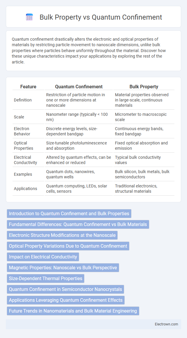
| Feature | Quantum Confinement | Bulk Property |
|---|---|---|
| Definition | Restriction of particle motion in one or more dimensions at nanoscale | Material properties observed in large-scale, continuous materials |
| Scale | Nanometer range (typically < 100 nm) | Micrometer to macroscopic scale |
| Electron Behavior | Discrete energy levels, size-dependent bandgap | Continuous energy bands, fixed bandgap |
| Optical Properties | Size-tunable photoluminescence and absorption | Fixed optical absorption and emission |
| Electrical Conductivity | Altered by quantum effects, can be enhanced or reduced | Typical bulk conductivity values |
| Examples | Quantum dots, nanowires, quantum wells | Bulk silicon, bulk metals, bulk semiconductors |
| Applications | Quantum computing, LEDs, solar cells, sensors | Traditional electronics, structural materials |
Introduction to Quantum Confinement and Bulk Properties
Quantum confinement occurs when the dimensions of a material are reduced to the nanoscale, typically below the exciton Bohr radius, causing discrete energy levels and altered electronic properties. In contrast, bulk properties represent the behavior of materials at macroscale dimensions where energy bands are continuous and electronic states are delocalized. This fundamental difference affects optical, electrical, and magnetic characteristics, enabling unique applications in nanotechnology and semiconductor devices.
Fundamental Differences: Quantum Confinement vs Bulk Materials
Quantum confinement occurs when the dimensions of a material are reduced to the nanoscale, typically below the exciton Bohr radius, causing electrons and holes to experience spatial restriction that alters electronic and optical properties. In bulk materials, electrons move freely within the continuous energy bands, resulting in well-defined bulk properties such as bandgap energies that remain constant regardless of size. Your understanding of these fundamental differences is essential for applications in nanotechnology and optoelectronics, where quantum confinement enables tunable material characteristics unattainable in bulk counterparts.
Electronic Structure Modifications at the Nanoscale
Quantum confinement significantly alters the electronic structure of materials by reducing their size to the nanoscale, leading to discrete energy levels rather than continuous bands observed in bulk properties. Electrons confined within nanoscale dimensions experience quantization effects, increasing bandgap energy and modifying optical and electrical behaviors compared to bulk counterparts. These electronic structure modifications enable tunable properties in semiconductor quantum dots, nanowires, and thin films essential for advanced optoelectronic and quantum computing applications.
Optical Property Variations Due to Quantum Confinement
Quantum confinement significantly alters the optical properties of materials compared to their bulk counterparts by causing discrete energy levels and size-dependent bandgap variations. Nanostructures, such as quantum dots, exhibit enhanced photoluminescence and tunable emission spectra due to electron and hole wavefunction confinement. This leads to higher quantum efficiency and wavelength shifts that are not present in bulk materials with continuous energy bands.
Impact on Electrical Conductivity
Quantum confinement significantly alters electrical conductivity by restricting electron movement to nanoscale dimensions, increasing energy band gaps compared to bulk materials. This confinement leads to discrete energy levels and reduced carrier mobility, which can enhance or diminish conductivity based on the material and size of the nanostructure. Your ability to tailor electrical properties through quantum confinement enables advanced applications in nanoelectronics and optoelectronics.
Magnetic Properties: Nanoscale vs Bulk Perspective
Magnetic properties at the nanoscale differ significantly from bulk materials due to quantum confinement effects that alter electron spin alignment and magnetic domain structures. In nanoscale materials, reduced dimensions enhance surface-to-volume ratios, often resulting in superparamagnetism or size-dependent magnetic anisotropy, unlike the stable ferromagnetic behavior seen in bulk counterparts. Understanding these changes is crucial for optimizing Your applications in spintronics, magnetic storage, and nanoscale sensors.
Size-Dependent Thermal Properties
Quantum confinement significantly alters the thermal properties of materials by restricting phonon transport in nanostructures, leading to reduced thermal conductivity compared to their bulk counterparts. As particle size decreases to the nanoscale, increased surface-to-volume ratio and boundary scattering dominate heat transfer mechanisms, resulting in size-dependent thermal behaviors. These effects enable the design of materials with tailored thermal conductivities for applications in thermoelectrics and nanoelectronics.
Quantum Confinement in Semiconductor Nanocrystals
Quantum confinement in semiconductor nanocrystals dramatically alters their electronic and optical properties compared to bulk materials by restricting electron movement to nanoscale dimensions. This confinement increases the bandgap energy, allowing tunable photoluminescence based on particle size, which is crucial for applications in LEDs, lasers, and solar cells. Understanding how quantum confinement affects your nanocrystal behavior enables precise control over device performance in advanced optoelectronic technologies.
Applications Leveraging Quantum Confinement Effects
Quantum confinement effects are crucial in the design of quantum dots used in high-efficiency photovoltaic cells and advanced display technologies, enabling tuning of electronic and optical properties at the nanoscale. In contrast to bulk materials, quantum-confined structures exhibit discrete energy levels that enhance charge carrier dynamics, improving device performance in lasers, sensors, and quantum computing components. Researchers exploit these effects to create nanoscale devices with tailored emission wavelengths and increased sensitivity, revolutionizing optoelectronics and nanomedicine applications.
Future Trends in Nanomaterials and Bulk Material Engineering
Quantum confinement significantly alters electronic and optical properties in nanomaterials compared to their bulk counterparts, enabling tailored functionalities for next-generation devices. Future trends in nanomaterials focus on exploiting size-dependent effects to enhance performance in areas like photovoltaics, sensors, and quantum computing. Bulk material engineering continues to evolve by integrating nanoscale components to create hybrid systems with improved mechanical strength, thermal stability, and multifunctionality.
quantum confinement vs bulk property Infographic