Deep UV Lithography offers high throughput and cost efficiency for patterning at the nanoscale, making it ideal for large-volume semiconductor manufacturing, while Electron Beam Lithography excels in achieving ultra-high resolution and flexibility for custom or low-volume applications. Discover how your choice between these techniques can impact precision, scalability, and overall project success in the rest of the article.
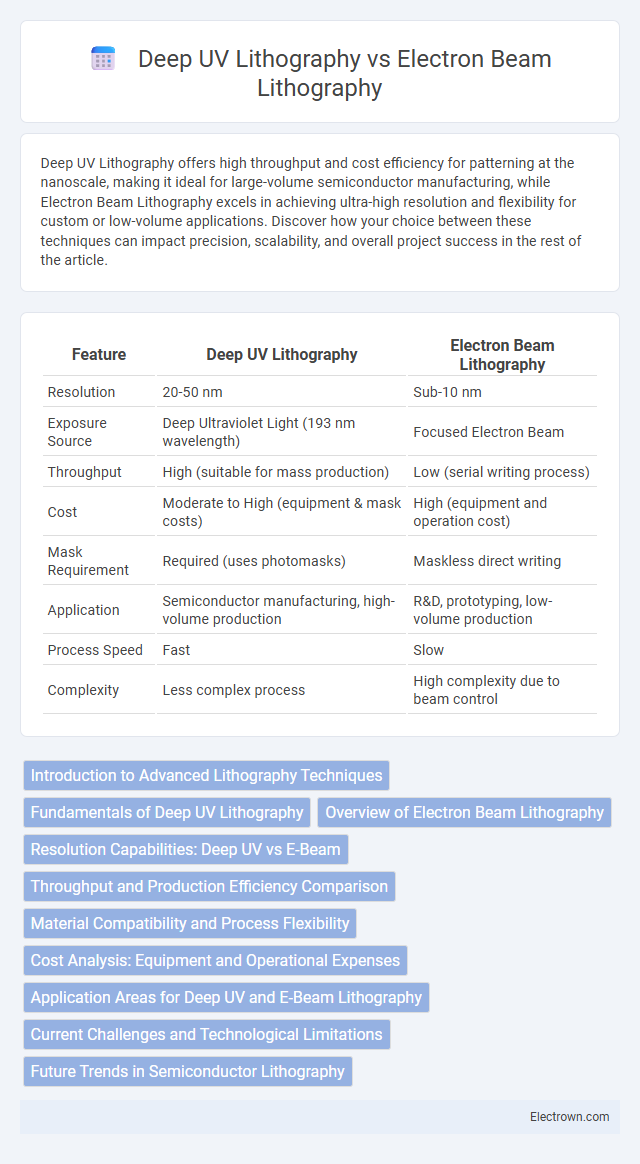
Table of Comparison
| Feature | Deep UV Lithography | Electron Beam Lithography |
|---|---|---|
| Resolution | 20-50 nm | Sub-10 nm |
| Exposure Source | Deep Ultraviolet Light (193 nm wavelength) | Focused Electron Beam |
| Throughput | High (suitable for mass production) | Low (serial writing process) |
| Cost | Moderate to High (equipment & mask costs) | High (equipment and operation cost) |
| Mask Requirement | Required (uses photomasks) | Maskless direct writing |
| Application | Semiconductor manufacturing, high-volume production | R&D, prototyping, low-volume production |
| Process Speed | Fast | Slow |
| Complexity | Less complex process | High complexity due to beam control |
Introduction to Advanced Lithography Techniques
Deep UV Lithography uses 193 nm wavelength light to pattern semiconductor features with high throughput and scalability for mass production. Electron Beam Lithography offers superior resolution down to sub-10 nm by directly writing patterns with a focused electron beam, ideal for prototyping and low-volume fabrication. Your choice between these advanced lithography techniques depends on balancing resolution requirements with cost and production volume.
Fundamentals of Deep UV Lithography
Deep UV lithography utilizes ultraviolet light with wavelengths typically around 193 nm or 248 nm to pattern semiconductor wafers in photolithography processes, enabling high-resolution image transfer through photomasks. This technique relies on photoresists sensitive to deep UV radiation, where exposure alters the resist's solubility, allowing selective removal and precise pattern definition. The fundamental advantage of Deep UV lithography lies in its ability to achieve sub-100 nm feature sizes with high throughput, making it essential for large-scale semiconductor manufacturing.
Overview of Electron Beam Lithography
Electron Beam Lithography (EBL) is a high-precision maskless lithography technique used for nanoscale patterning, employing a focused beam of electrons to directly write patterns onto a resist-coated substrate. Unlike Deep UV Lithography, EBL offers superior resolution below 10 nm, making it ideal for research and prototype fabrication in semiconductor manufacturing and nanotechnology. You can achieve intricate, customizable designs without the need for photomasks, though EBL has slower throughput and higher operational costs compared to Deep UV Lithography.
Resolution Capabilities: Deep UV vs E-Beam
Deep UV lithography typically achieves resolution down to 38 nm using 193 nm wavelength light sources and advanced immersion techniques, while electron beam lithography (E-beam) can reach sub-10 nm resolution due to direct electron exposure without mask limitations. The superior resolution of E-beam lithography makes it ideal for prototype semiconductor devices and high-precision nanofabrication, despite slower throughput compared to Deep UV. Deep UV lithography remains dominant in high-volume manufacturing where resolutions around 20-30 nm are standard by leveraging advanced photomasks and multiple patterning strategies.
Throughput and Production Efficiency Comparison
Deep UV lithography offers significantly higher throughput than electron beam lithography due to its parallel exposure process using photomasks, enabling efficient mass production of semiconductor devices. Electron beam lithography, while highly precise and ideal for prototyping or small-volume production, suffers from slow serial writing speeds that limit its production efficiency in large-scale manufacturing. This throughput disparity makes deep UV lithography the preferred technology for high-volume semiconductor fabs focused on rapid and cost-effective wafer processing.
Material Compatibility and Process Flexibility
Deep UV lithography offers broad material compatibility due to its reliance on optical exposure, enabling efficient patterning of photoresists on various semiconductor substrates like silicon, gallium arsenide, and flexible polymers. Electron beam lithography provides exceptional process flexibility with direct-write capabilities, allowing precise patterning on diverse materials including metals, insulators, and resist layers without masks, ideal for prototyping and complex designs. Your choice depends on whether you prioritize throughput and material versatility with Deep UV or the high-resolution and customizable exposure of Electron Beam Lithography.
Cost Analysis: Equipment and Operational Expenses
Deep UV lithography involves high initial equipment costs due to sophisticated light sources and photomask fabrication but offers faster throughput, reducing operational expenses over time. Electron beam lithography requires lower equipment investment but incurs higher operational costs from slower processing speeds and frequent maintenance of electron sources. Your choice hinges on balancing upfront capital against long-term operational efficiency for semiconductor manufacturing.
Application Areas for Deep UV and E-Beam Lithography
Deep UV lithography is extensively used in mass semiconductor manufacturing, particularly for fabricating integrated circuits with feature sizes down to 7 nm due to its high throughput and cost-efficiency. Electron beam lithography excels in mask making, prototyping, and research environments, offering ultra-high resolution patterning below 10 nm but with slower write speeds unsuitable for large-scale production. Applications of e-beam lithography include nanophotonics, quantum devices, and specialized nanostructures where precision outweighs throughput constraints.
Current Challenges and Technological Limitations
Deep UV lithography faces challenges in achieving feature sizes below 20 nm due to wavelength limits and mask defects, while electron beam lithography struggles with slow write speeds and high costs, limiting mass production scalability. Both technologies encounter difficulties in resist sensitivity and pattern uniformity, impacting yield and device performance. Your choice depends on balancing throughput needs versus resolution precision for next-generation semiconductor manufacturing.
Future Trends in Semiconductor Lithography
Future trends in semiconductor lithography emphasize the evolution of Deep UV lithography with Extreme Ultraviolet (EUV) technology providing higher resolution and throughput for mass production. Electron Beam Lithography (EBL) continues advancing with multi-beam systems to enhance speed and precision for prototyping and low-volume manufacturing. Your choice between these methods should consider scalability, cost, and the intricate demands of next-generation semiconductor devices.
Deep UV Lithography vs Electron Beam Lithography Infographic