2D material FETs exhibit superior electrostatic control, reduced short-channel effects, and enhanced carrier mobility compared to bulk material FETs, enabling more efficient and scalable device performance. Explore the rest of the article to understand how these differences impact the future of semiconductor technology and your applications.
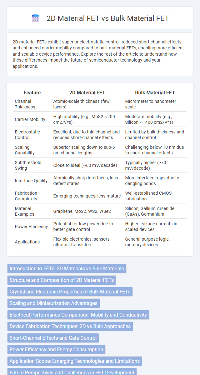
Table of Comparison
| Feature | 2D Material FET | Bulk Material FET |
|---|---|---|
| Channel Thickness | Atomic-scale thickness (few layers) | Micrometer to nanometer scale |
| Carrier Mobility | High mobility (e.g., MoS2 ~200 cm2/V*s) | Moderate mobility (e.g., Silicon ~1400 cm2/V*s) |
| Electrostatic Control | Excellent, due to thin channel and reduced short-channel effects | Limited by bulk thickness and channel control |
| Scaling Capability | Superior scaling down to sub-5 nm channel lengths | Challenging below 10 nm due to short-channel effects |
| Subthreshold Swing | Close to ideal (~60 mV/decade) | Typically higher (>70 mV/decade) |
| Interface Quality | Atomically sharp interfaces, less defect states | More interface traps due to dangling bonds |
| Fabrication Complexity | Emerging techniques, less mature | Well-established CMOS fabrication |
| Material Examples | Graphene, MoS2, WS2, WSe2 | Silicon, Gallium Arsenide (GaAs), Germanium |
| Power Efficiency | Potential for low power due to better gate control | Higher leakage currents in scaled devices |
| Applications | Flexible electronics, sensors, ultrafast transistors | General-purpose logic, memory devices |
Introduction to FETs: 2D Materials vs Bulk Materials
Field-effect transistors (FETs) based on 2D materials such as graphene, transition metal dichalcogenides (TMDs), and black phosphorus exhibit superior electrostatic control and reduced short-channel effects compared to bulk material FETs, enabling enhanced device scaling and performance. Unlike bulk material FETs that rely on three-dimensional semiconductor substrates like silicon, 2D material FETs utilize atomically thin layers with high carrier mobility and flexibility, offering new opportunities for ultra-thin, transparent, and flexible electronics. The absence of dangling bonds and reduced interface trap density in 2D materials improve device reliability and switching characteristics, distinguishing them from conventional bulk semiconductor devices.
Structure and Composition of 2D Material FETs
2D Material Field-Effect Transistors (FETs) feature atomically thin semiconductor channels composed of layered materials such as graphene, transition metal dichalcogenides (TMDs), or black phosphorus, contrasting with the thicker, three-dimensional bulk semiconductor channels in conventional FETs. The ultrathin, planar structure of 2D materials allows for superior electrostatic control and reduced short-channel effects, enhancing device performance. Your choice of a 2D material FET can significantly impact scalability and flexibility due to its unique composition and layered structure.
Crystal and Electronic Properties of Bulk Material FETs
Bulk material FETs typically utilize three-dimensional crystals with indirect bandgaps and strong interlayer coupling, which results in lower carrier mobility and increased scattering compared to 2D materials. The bulk crystal structure leads to a higher density of trap states and defects, negatively impacting electronic performance such as subthreshold swing and ON/OFF current ratios. Due to the presence of bulk defects and reduced electrostatic gate control, bulk material FETs often exhibit higher power consumption and limited scalability in nanoelectronic applications.
Scaling and Miniaturization Advantages
2D material FETs exhibit superior scaling and miniaturization advantages compared to bulk material FETs due to their atomic-scale thickness, which reduces short-channel effects and enables aggressive channel length scaling below 5 nm. The atomically flat and defect-free interface in 2D materials enhances carrier mobility and electrostatic control, supporting higher device density and improved performance at nanoscale dimensions. These properties make 2D material FETs highly suitable for advanced semiconductor nodes where traditional bulk FET scaling faces fundamental physical limitations.
Electrical Performance Comparison: Mobility and Conductivity
2D material FETs exhibit significantly higher carrier mobility compared to bulk material FETs, often exceeding values of 1000 cm2/V*s in materials like MoS2 and graphene, which enhances electron transport efficiency. The atomic thinness of 2D materials reduces scattering and allows for better electrostatic control, resulting in improved conductivity and on/off current ratios. In contrast, bulk material FETs suffer from lower mobility due to increased impurity scattering and substrate effects, limiting their electrical performance in high-speed applications.
Device Fabrication Techniques: 2D vs Bulk Approaches
Device fabrication techniques for 2D material FETs emphasize precise layer transfer, exfoliation, or chemical vapor deposition (CVD) to achieve atomically thin channels, contrasting with bulk material FETs that primarily rely on traditional photolithography and doping methods in silicon wafers. The 2D approach demands ultra-clean interfaces and often involves van der Waals heterostructures, while bulk FET fabrication integrates well-established processes like ion implantation and thermal oxidation for gate dielectric formation. Scalability challenges in 2D FETs stem from uniform material synthesis and transfer precision, whereas bulk FETs benefit from mature, high-throughput semiconductor manufacturing infrastructure.
Short-Channel Effects and Gate Control
2D Material FETs exhibit superior gate control compared to Bulk Material FETs due to atomic-scale thickness, which effectively suppresses short-channel effects such as drain-induced barrier lowering and punch-through. The reduced dimensionality in 2D materials allows for better electrostatic integrity, enabling device scaling down to sub-10 nm channel lengths without significant performance degradation. Your choice of 2D Material FET can significantly enhance device reliability and scaling in advanced semiconductor applications.
Power Efficiency and Energy Consumption
2D material FETs exhibit superior power efficiency compared to bulk material FETs due to their atomically thin channels, which reduce short-channel effects and enable lower operating voltages. The reduced dimensionality in 2D FETs minimizes leakage currents, significantly lowering energy consumption during switching events. Your choice of 2D material transistors can lead to enhanced performance in low-power electronic applications, making them ideal for energy-sensitive devices.
Application Scope: Emerging Technologies and Limitations
2D material FETs show exceptional potential in emerging technologies such as flexible electronics, high-speed transistors, and nanoscale sensors due to their atomic thickness and superior electrostatic control. Bulk material FETs, while well-established in conventional integrated circuits, face limitations in scaling down beyond sub-10 nm nodes, leading to short-channel effects and performance bottlenecks. The atomically thin nature of 2D materials enables reduced short-channel effects and enhanced carrier mobility, overcoming bulk material FET constraints for next-generation device applications.
Future Perspectives and Challenges in FET Development
2D material FETs offer superior electrostatic control and scalability compared to bulk material FETs, enabling continued device miniaturization and enhanced performance for next-generation electronics. Challenges in 2D FET development include achieving large-area synthesis with high purity, reliable contact engineering, and stability under ambient conditions. Future perspectives emphasize integration with current CMOS technology, exploring novel 2D heterostructures, and overcoming variability issues to realize practical applications in flexible, low-power, and high-speed devices.
2D Material FET vs Bulk Material FET Infographic