Intercalation and doping are two key methods to modify the electronic properties of 2D materials, where intercalation involves inserting molecules or ions between layers, while doping refers to introducing impurity atoms within the lattice. Understanding these processes can significantly enhance your ability to tailor material performance for specific applications; explore the article further to grasp the detailed mechanisms and effects.
Table of Comparison
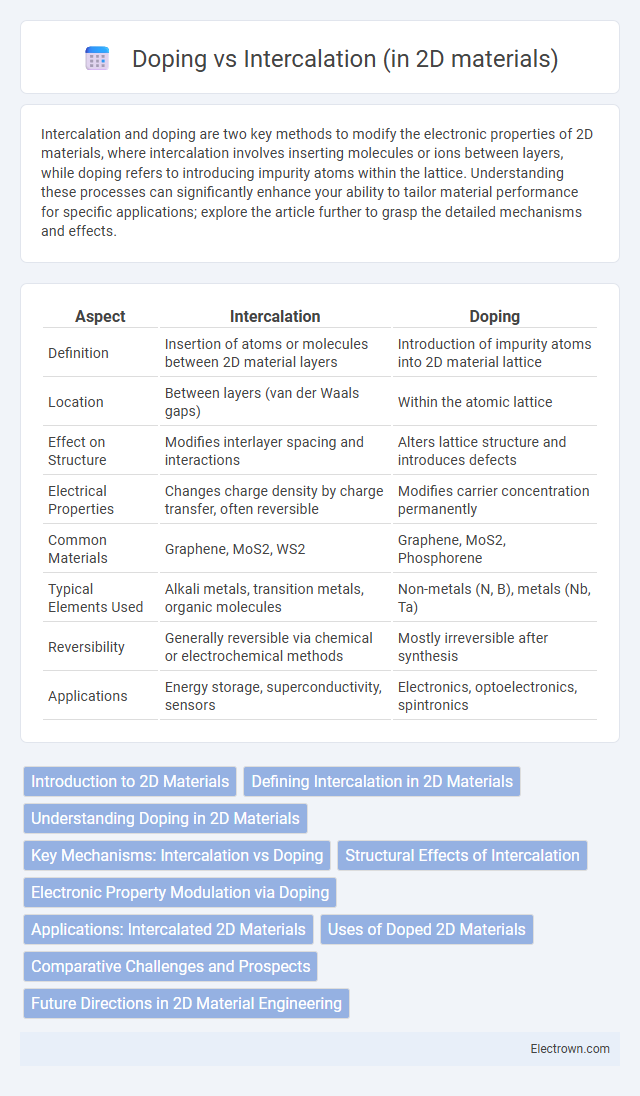
| Aspect | Intercalation | Doping |
|---|---|---|
| Definition | Insertion of atoms or molecules between 2D material layers | Introduction of impurity atoms into 2D material lattice |
| Location | Between layers (van der Waals gaps) | Within the atomic lattice |
| Effect on Structure | Modifies interlayer spacing and interactions | Alters lattice structure and introduces defects |
| Electrical Properties | Changes charge density by charge transfer, often reversible | Modifies carrier concentration permanently |
| Common Materials | Graphene, MoS2, WS2 | Graphene, MoS2, Phosphorene |
| Typical Elements Used | Alkali metals, transition metals, organic molecules | Non-metals (N, B), metals (Nb, Ta) |
| Reversibility | Generally reversible via chemical or electrochemical methods | Mostly irreversible after synthesis |
| Applications | Energy storage, superconductivity, sensors | Electronics, optoelectronics, spintronics |
Introduction to 2D Materials
2D materials, characterized by their atomic-scale thickness and high surface area, exhibit unique electronic, optical, and mechanical properties essential for advanced applications. Intercalation involves inserting guest species between layers, modifying properties without disrupting the 2D lattice, while doping introduces impurities directly into the lattice to tailor electrical conductivity and carrier concentration. Your choice between intercalation and doping depends on the desired alteration of the 2D material's performance for applications like sensors, energy storage, or electronics.
Defining Intercalation in 2D Materials
Intercalation in 2D materials involves inserting guest atoms, ions, or molecules between the layers without significantly disturbing the host lattice structure, enhancing properties like conductivity and ion storage. This process differs fundamentally from doping, which introduces impurities directly into the lattice to modify electrical characteristics. Understanding intercalation allows you to tailor 2D materials for applications in energy storage, electronics, and catalysis by controlling layer spacing and electronic interactions.
Understanding Doping in 2D Materials
Doping in 2D materials involves introducing impurities to modulate electrical properties by altering carrier concentration, enhancing conductivity, and enabling tunable semiconductor behavior. Common dopants include atoms like nitrogen or boron in graphene and transition metal dichalcogenides (TMDs), which shift Fermi levels and affect charge transport characteristics. Unlike intercalation, which inserts species between layers without substitution, doping directly modifies the lattice structure or electronic environment to tailor device performance in sensors, transistors, and optoelectronics.
Key Mechanisms: Intercalation vs Doping
Intercalation in 2D materials involves the insertion of guest species between atomic layers, altering electronic properties by modulating interlayer spacing and charge transfer. Doping, on the other hand, introduces impurity atoms directly into the crystal lattice, modifying carrier concentration and mobility within the material. Your choice between these methods depends on the desired control over electronic behavior and structural integrity in applications like sensors or energy storage devices.
Structural Effects of Intercalation
Intercalation in 2D materials involves inserting guest atoms or molecules between layers, causing lattice expansion and altered interlayer spacing, which can significantly modify electronic and mechanical properties. This structural modification contrasts with doping, where foreign atoms replace or occupy sites within the lattice without altering the interlayer spacing drastically. Understanding these structural effects of intercalation enables you to tailor material characteristics for applications in energy storage and nanoelectronics.
Electronic Property Modulation via Doping
Doping in 2D materials involves introducing impurity atoms to modulate electronic properties, enhancing conductivity, carrier concentration, and creating n-type or p-type semiconductors. Intercalation, by contrast, inserts molecules or ions between layers, influencing charge transfer but often with less precision in tuning carrier density compared to doping. You can achieve more tailored electronic property modulation through doping, crucial for optimizing device performance in electronics and optoelectronics based on 2D materials.
Applications: Intercalated 2D Materials
Intercalated 2D materials exhibit enhanced electronic, magnetic, and catalytic properties, making them ideal for energy storage devices such as batteries and supercapacitors, where improved ion diffusion and charge capacity are critical. In electrochemical sensors, intercalation tailors sensitivity and selectivity by modulating the electronic structure and surface chemistry of 2D materials like graphene and transition metal dichalcogenides (TMDs). These materials also find applications in spintronics and superconductivity, where intercalated species introduce novel magnetic and conductive phases unattainable through doping.
Uses of Doped 2D Materials
Doped 2D materials exhibit enhanced electrical conductivity, making them ideal for applications in flexible electronics, sensors, and energy storage devices. Your ability to fine-tune the electronic properties through doping enables improvements in catalytic activity and charge carrier concentration, essential for high-performance transistors and battery electrodes. These tailored modifications expand the functionality of 2D materials in next-generation optoelectronic and nanoelectronic systems.
Comparative Challenges and Prospects
Intercalation in 2D materials involves inserting ions or molecules between layers, presenting challenges in maintaining structural integrity and achieving uniform distribution, while doping introduces impurities directly into the lattice, often risking defects that impair electronic properties. Both techniques aim to tailor electrical and optical characteristics, but intercalation offers reversible tuning with potential for energy storage applications, whereas doping provides more permanent modifications suitable for semiconductor devices. Your choice depends on balancing the need for stability, controllability, and device function in applications such as sensors, transistors, or batteries.
Future Directions in 2D Material Engineering
Future directions in 2D material engineering focus on enhancing electronic properties through precise intercalation and doping techniques, which tailor conductivity, carrier concentration, and chemical reactivity. Intercalation introduces guest species between layers to modulate interlayer spacing and charge transfer, while doping integrates foreign atoms into the lattice to create localized states and modify band structure. Your advancements in controlled intercalation and doping processes will drive innovation in flexible electronics, sensors, and energy storage applications.
Intercalation vs Doping (in 2D materials) Infographic