Electron beam lithography offers unparalleled precision for nanoscale patterning, surpassing photolithography's resolution limits but at a slower throughput and higher cost. Explore the rest of the article to understand which technique best suits your semiconductor fabrication needs.
Table of Comparison
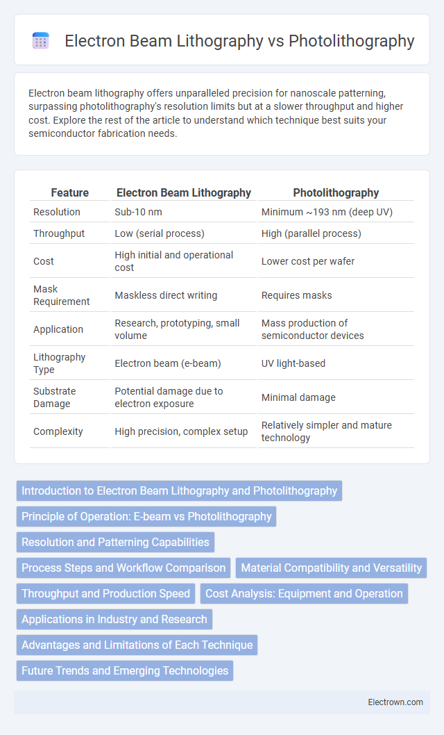
| Feature | Electron Beam Lithography | Photolithography |
|---|---|---|
| Resolution | Sub-10 nm | Minimum ~193 nm (deep UV) |
| Throughput | Low (serial process) | High (parallel process) |
| Cost | High initial and operational cost | Lower cost per wafer |
| Mask Requirement | Maskless direct writing | Requires masks |
| Application | Research, prototyping, small volume | Mass production of semiconductor devices |
| Lithography Type | Electron beam (e-beam) | UV light-based |
| Substrate Damage | Potential damage due to electron exposure | Minimal damage |
| Complexity | High precision, complex setup | Relatively simpler and mature technology |
Introduction to Electron Beam Lithography and Photolithography
Electron beam lithography (EBL) uses a focused beam of electrons to create extremely precise patterns on a substrate, enabling nanoscale feature fabrication crucial for semiconductor device prototyping and advanced research. Photolithography employs ultraviolet light through a photomask to transfer patterns onto photoresist-coated wafers, widely utilized in mass production of integrated circuits due to its high throughput and cost efficiency. Both techniques are fundamental in semiconductor manufacturing, with EBL excelling in resolution and flexibility, while photolithography offers scalability for large-volume production.
Principle of Operation: E-beam vs Photolithography
Electron beam lithography operates by directing a focused beam of electrons to precisely pattern a resist-coated substrate at the nanometer scale, enabling high-resolution and maskless patterning. Photolithography utilizes ultraviolet light passed through a photomask to transfer geometric patterns onto a photosensitive resist, offering faster processing over larger areas but with resolution limits imposed by the wavelength of light. The fundamental difference lies in E-beam's direct-write, maskless method driven by electron interactions, whereas photolithography relies on optical exposure through masks for pattern transfer.
Resolution and Patterning Capabilities
Electron beam lithography offers superior resolution, achieving feature sizes below 10 nanometers due to its direct-write process using focused electron beams. Photolithography, limited by the diffraction limit of light, typically achieves minimum feature sizes around 20-40 nanometers with advanced immersion and EUV techniques. Electron beam lithography excels in complex, high-precision patterning for prototyping and nanoscale device fabrication, while photolithography remains optimal for high-throughput production with less intricate pattern requirements.
Process Steps and Workflow Comparison
Electron beam lithography involves direct writing of patterns onto a resist-coated substrate using a focused electron beam, enabling high-resolution patterning without masks, but with slower throughput due to serial exposure. Photolithography utilizes ultraviolet light to project patterns through a photomask onto a photoresist layer, allowing rapid, parallel processing suited for large-scale manufacturing but limited by diffraction effects affecting resolution. Workflow in electron beam lithography typically includes resist coating, electron beam exposure, development, and etching, whereas photolithography incorporates mask alignment, UV exposure, resist development, and etching in a more streamlined, high-throughput process.
Material Compatibility and Versatility
Electron beam lithography offers superior material compatibility by directly writing patterns onto a wide range of substrates, including non-planar and sensitive materials, without requiring masks. Photolithography excels in versatility for high-volume semiconductor manufacturing, efficiently processing standard photoresists on silicon wafers but faces limitations with complex or unconventional materials. The choice between these techniques depends heavily on the specific material properties and the design flexibility required for the application.
Throughput and Production Speed
Electron beam lithography offers high precision but suffers from lower throughput and slower production speed due to its serial writing process. Photolithography excels in mass production environments, providing significantly faster exposure times and higher throughput by patterning entire wafers simultaneously. Your choice depends on whether precision or rapid volume manufacturing is the priority.
Cost Analysis: Equipment and Operation
Electron beam lithography incurs higher initial equipment costs, often exceeding several hundred thousand dollars due to advanced electron optics and vacuum systems, making it substantially more expensive than photolithography, whose equipment can range from tens to a few hundred thousand dollars depending on system complexity. Operational expenses for electron beam lithography remain elevated because of slower writing speeds and higher maintenance demands, whereas photolithography benefits from faster throughput and established process automation, significantly reducing per-unit production costs in high-volume manufacturing. The cost-effectiveness of photolithography favors large-scale semiconductor fabrication, while electron beam lithography is economically viable for low-volume, high-resolution prototyping and research applications.
Applications in Industry and Research
Electron beam lithography offers unmatched resolution for fabricating nanoscale devices, making it essential in semiconductor research, quantum computing, and advanced nanofabrication industries. Photolithography dominates high-volume semiconductor manufacturing due to its speed and scalability, underpinning integrated circuit production in consumer electronics and MEMS devices. Both techniques complement each other: electron beam lithography excels in prototyping and custom nanostructures, while photolithography drives mass production of microchips and photonic components.
Advantages and Limitations of Each Technique
Electron beam lithography offers unmatched resolution down to sub-10 nanometers, making it ideal for creating complex nanoscale patterns with high precision, but its slow throughput and high cost limit large-scale manufacturing. Photolithography excels in high-volume semiconductor production due to its rapid processing and cost-effectiveness, yet it struggles to achieve features below 20 nanometers because of diffraction limits. Your choice depends on whether ultra-fine detail or mass production efficiency is the priority in your application.
Future Trends and Emerging Technologies
Future trends in electron beam lithography (EBL) and photolithography highlight advancements like extreme ultraviolet (EUV) lithography enhancing photolithography resolution beyond 7 nm nodes, while EBL explores multi-beam systems to increase throughput for maskless patterning. Emerging technologies such as directed self-assembly (DSA) complement both techniques by enabling finer feature definitions and defect reduction in semiconductor manufacturing. Your choice between EBL and photolithography will depend on balancing ultimate resolution needs with scalability for next-generation integrated circuits.
Electron beam lithography vs Photolithography Infographic