Schottky junctions feature a metal-semiconductor interface offering faster switching speeds and lower forward voltage drops compared to p-n junctions, which utilize semiconductor-semiconductor contacts for better reverse-bias voltage handling and higher breakdown voltages. Explore the detailed differences and applications to understand which junction best suits your electronic device needs.
Table of Comparison
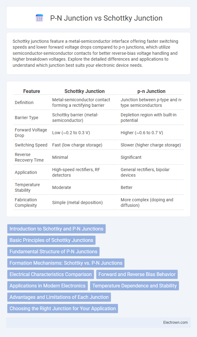
| Feature | Schottky Junction | p-n Junction |
|---|---|---|
| Definition | Metal-semiconductor contact forming a rectifying barrier | Junction between p-type and n-type semiconductors |
| Barrier Type | Schottky barrier (metal-semiconductor) | Depletion region with built-in potential |
| Forward Voltage Drop | Low (~0.2 to 0.3 V) | Higher (~0.6 to 0.7 V) |
| Switching Speed | Fast (low charge storage) | Slower (higher charge storage) |
| Reverse Recovery Time | Minimal | Significant |
| Application | High-speed rectifiers, RF detectors | General rectifiers, bipolar devices |
| Temperature Stability | Moderate | Better |
| Fabrication Complexity | Simple (metal deposition) | More complex (doping and diffusion) |
Introduction to Schottky and P-N Junctions
Schottky junctions form at the interface between a metal and a semiconductor, creating a rectifying contact characterized by a low forward voltage drop and fast switching speeds. P-N junctions consist of p-type and n-type semiconductor materials joined together, enabling charge carrier diffusion and the formation of a depletion region that controls current flow. Understanding the differences in their conduction mechanisms and barrier properties helps optimize Your electronic device design for specific applications.
Basic Principles of Schottky Junctions
Schottky junctions form at the interface between a metal and a semiconductor, creating a rectifying barrier due to the difference in work functions, which controls electron flow with minimal minority carrier injection. Unlike p-n junctions that rely on the charge depletion region between p-type and n-type semiconductors, Schottky barriers facilitate faster switching speeds and lower forward voltage drops. Understanding these basic principles helps you optimize device performance in high-speed and low-power applications.
Fundamental Structure of P-N Junctions
The fundamental structure of p-n junctions consists of adjacent p-type and n-type semiconductor regions creating a depletion zone where charge carriers recombine, establishing an electric field that controls current flow. Unlike Schottky junctions formed at metal-semiconductor interfaces, p-n junctions rely on the diffusion of holes and electrons across the semiconductor junction, generating a built-in potential barrier. Your electronic devices benefit from p-n junctions due to their ability to efficiently rectify current and serve as the basis for diodes, transistors, and solar cells.
Formation Mechanisms: Schottky vs. P-N Junctions
Schottky junctions form at the interface between a metal and a semiconductor, where the difference in work functions creates a potential barrier affecting charge carrier flow. P-N junctions arise from the contact of p-type and n-type semiconductors, creating a depletion region due to diffusion of electrons and holes and the establishment of an electric field. The distinct formation mechanisms lead to Schottky junctions having faster switching speeds and lower forward voltage drops compared to the broader charge carrier recombination processes in p-n junctions.
Electrical Characteristics Comparison
Schottky junctions exhibit lower forward voltage drop, typically around 0.2 to 0.3 volts, compared to 0.7 volts in p-n junctions, resulting in higher efficiency and faster switching speeds due to minimal charge storage. Reverse leakage current in Schottky diodes is generally higher than in p-n junction diodes, which impacts their suitability in high-voltage applications. The ideality factor for Schottky junctions tends to be closer to 1, indicating near-ideal diode behavior, while p-n junctions often have higher ideality factors due to recombination mechanisms within the depletion region.
Forward and Reverse Bias Behavior
Schottky junctions exhibit lower forward voltage drop (typically 0.2 to 0.3 V) compared to p-n junctions (around 0.7 V), enabling faster switching and higher efficiency in forward bias. Under reverse bias, Schottky diodes generally have higher leakage currents due to the metal-semiconductor interface, whereas p-n junctions offer better reverse voltage blocking and lower leakage currents due to depletion region properties. The absence of minority carrier injection in Schottky junctions leads to reduced charge storage, resulting in minimal reverse recovery time, in contrast to p-n junctions which experience significant charge storage and slower switching speeds.
Applications in Modern Electronics
Schottky junctions excel in high-speed switching and low forward voltage drop applications, making them ideal for power rectifiers, radio frequency devices, and high-frequency mixers in modern electronics. P-n junctions are widely utilized in diodes, transistors, solar cells, and LED technology, offering efficient charge carrier separation and amplification for integrated circuits. The distinct barrier characteristics of Schottky and p-n junctions influence their roles, with Schottky favored for fast response and low power loss, while p-n junctions are preferred for voltage regulation and signal processing.
Temperature Dependence and Stability
Schottky junctions exhibit lower temperature dependence due to metal-semiconductor contacts that maintain stable barrier heights over a wide temperature range, enhancing device reliability. In contrast, p-n junctions show greater sensitivity to temperature variations, as thermal generation of charge carriers influences their forward and reverse bias characteristics, potentially leading to increased leakage currents. Stability in Schottky junctions is generally superior under thermal stress, making them preferred for high-temperature applications compared to conventional p-n junctions.
Advantages and Limitations of Each Junction
Schottky junctions offer faster switching speeds and lower forward voltage drops compared to p-n junctions, making them ideal for high-frequency and low-power applications. However, Schottky diodes exhibit higher reverse leakage currents and lower breakdown voltages, which can limit their use in high-voltage environments. You should consider p-n junctions for better thermal stability and higher reverse voltage tolerance, despite their slower switching characteristics and larger forward voltage drops.
Choosing the Right Junction for Your Application
Schottky junctions offer faster switching speeds and lower forward voltage drops, making them ideal for high-frequency and low-power applications like power rectifiers and RF circuits. P-n junctions provide better reverse voltage handling and higher breakdown voltage, suitable for applications requiring high-voltage tolerance and precise control, such as solar cells and diodes in power electronics. Your choice depends on balancing speed and efficiency needs against voltage and current requirements.
Schottky junction vs p-n junction Infographic