Lateral device structures offer simplified fabrication and efficient heat dissipation, making them ideal for low-power applications, while vertical device structures provide higher current densities and better performance in high-power electronics due to their compact design. Explore the rest of the article to understand which device structure best suits your technology needs.
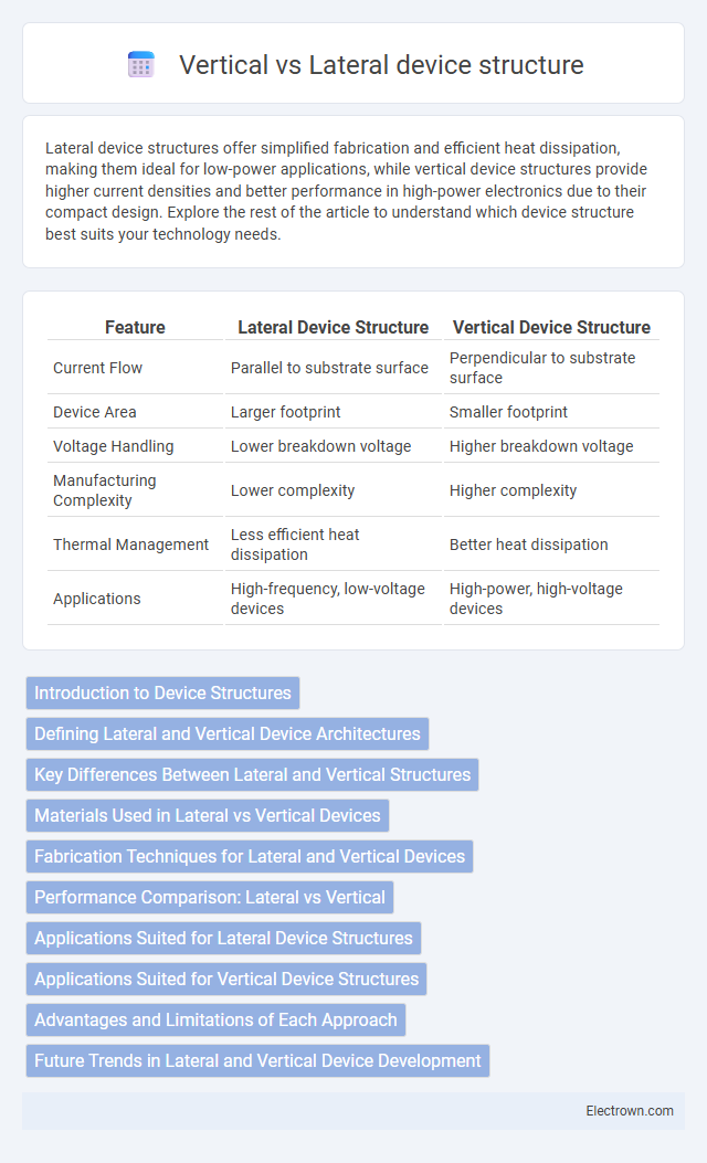
Table of Comparison
| Feature | Lateral Device Structure | Vertical Device Structure |
|---|---|---|
| Current Flow | Parallel to substrate surface | Perpendicular to substrate surface |
| Device Area | Larger footprint | Smaller footprint |
| Voltage Handling | Lower breakdown voltage | Higher breakdown voltage |
| Manufacturing Complexity | Lower complexity | Higher complexity |
| Thermal Management | Less efficient heat dissipation | Better heat dissipation |
| Applications | High-frequency, low-voltage devices | High-power, high-voltage devices |
Introduction to Device Structures
Lateral and vertical device structures differ primarily in current flow and fabrication layout, impacting performance and integration. Lateral devices feature horizontal current flow across the substrate surface, enabling simplified planar processing and ease of integration in ICs. Vertical devices allow current to flow perpendicularly through the substrate, providing higher current density and better heat dissipation for power applications.
Defining Lateral and Vertical Device Architectures
Lateral device architectures position the current flow parallel to the wafer surface, optimizing heat dissipation and enabling efficient integration in high-frequency applications. Vertical device structures direct current flow perpendicular through the wafer thickness, allowing higher power densities and improved breakdown voltages for power electronics. Understanding the fundamental differences between lateral and vertical architectures is essential for selecting the appropriate device design in semiconductor manufacturing and circuit applications.
Key Differences Between Lateral and Vertical Structures
Lateral device structures feature current flow parallel to the substrate surface, enabling easy integration with planar circuits and simplified fabrication processes, whereas vertical device structures have current flowing perpendicular to the substrate, supporting higher current densities and better heat dissipation. Lateral designs typically offer lower breakdown voltages and are preferred for low-power applications, while vertical designs excel in high-power, high-voltage environments due to their thicker drift regions and robust avalanche capability. The choice between lateral and vertical structures crucially impacts device performance metrics such as on-resistance, switching speed, and thermal management.
Materials Used in Lateral vs Vertical Devices
Lateral device structures often utilize silicon carbide (SiC) substrates with epitaxial layers for improved electron mobility and thermal management, while vertical devices commonly employ bulk SiC or gallium nitride (GaN) substrates to handle higher voltage and current densities. In lateral devices, materials such as AlGaN/GaN heterostructures are prevalent, enabling high electron mobility transistor (HEMT) performance on insulating substrates. Vertical devices rely on thick drift layers of SiC or GaN, optimizing breakdown voltage and power efficiency in high-voltage power electronics.
Fabrication Techniques for Lateral and Vertical Devices
Lateral device structures are typically fabricated using planar processes such as photolithography, ion implantation, and etching on a semiconductor surface, facilitating precise control over channel dimensions and alignment. Vertical device structures often require complex epitaxial growth, deep trench etching, and selective deposition techniques to build multilayer stacks with vertical current flow paths for enhanced device density. Advanced fabrication methods like atomic layer deposition (ALD) and chemical-mechanical polishing (CMP) play critical roles in achieving high-quality interfaces and minimizing defects in both lateral and vertical device architectures.
Performance Comparison: Lateral vs Vertical
Lateral device structures offer superior high-frequency performance due to shorter channel lengths and reduced parasitic capacitances, making them ideal for RF and microwave applications. Vertical device structures excel in power handling and thermal dissipation, supporting higher current densities and voltage ratings in power electronics. Your choice depends on whether you prioritize speed and integration density (lateral) or power efficiency and robustness (vertical).
Applications Suited for Lateral Device Structures
Lateral device structures are ideal for high-frequency and low-power applications due to their efficient heat dissipation and simpler fabrication processes. These structures are commonly used in RF amplifiers, analog circuits, and integrated power management systems where compact layout and low parasitic capacitance are crucial. Their planar design enables easy integration with other semiconductor components, making them favorable for mixed-signal and CMOS technologies.
Applications Suited for Vertical Device Structures
Vertical device structures are ideal for high-power and high-frequency applications due to their superior current handling and thermal management capabilities. They are commonly used in power electronics, such as insulated gate bipolar transistors (IGBTs) and vertical metal-oxide-semiconductor field-effect transistors (MOSFETs) for electric vehicles, industrial motor drives, and renewable energy systems. Choosing vertical structures ensures your devices achieve enhanced efficiency and reliability in demanding operational environments.
Advantages and Limitations of Each Approach
Lateral device structures offer advantages such as easier integration with planar technologies and improved thermal management due to their horizontal layout, but they face limitations in current handling and device scaling. Vertical device structures provide superior current density and smaller chip footprints, benefiting high-power and high-frequency applications, though they often involve more complex fabrication processes and higher manufacturing costs. Understanding these trade-offs helps you select the optimal device structure based on application requirements and performance criteria.
Future Trends in Lateral and Vertical Device Development
Future trends in lateral device development emphasize scaling down channel lengths and integrating advanced materials like 2D semiconductors to enhance electron mobility. Vertical devices are increasingly focused on three-dimensional integration, enabling higher current densities and improved thermal management through stacked architectures. Both structures leverage advancements in fabrication techniques, such as atomic layer deposition and nanoimprint lithography, to boost device performance and efficiency in emerging applications like AI and IoT.
Lateral vs Vertical device structure Infographic