Isolation trench and LOCOS isolation are semiconductor fabrication techniques used to electrically separate device components; isolation trenches offer superior scalability and reduced subthreshold leakage compared to LOCOS, which can suffer from bird's beak effects and limited scaling for advanced technologies. Discover how these differences impact your device performance and manufacturing choices by reading the full article.
Table of Comparison
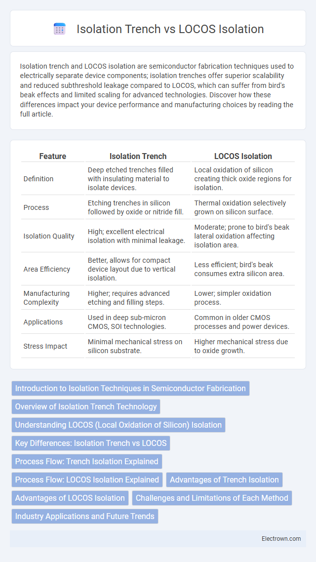
| Feature | Isolation Trench | LOCOS Isolation |
|---|---|---|
| Definition | Deep etched trenches filled with insulating material to isolate devices. | Local oxidation of silicon creating thick oxide regions for isolation. |
| Process | Etching trenches in silicon followed by oxide or nitride fill. | Thermal oxidation selectively grown on silicon surface. |
| Isolation Quality | High; excellent electrical isolation with minimal leakage. | Moderate; prone to bird's beak lateral oxidation affecting isolation area. |
| Area Efficiency | Better, allows for compact device layout due to vertical isolation. | Less efficient; bird's beak consumes extra silicon area. |
| Manufacturing Complexity | Higher; requires advanced etching and filling steps. | Lower; simpler oxidation process. |
| Applications | Used in deep sub-micron CMOS, SOI technologies. | Common in older CMOS processes and power devices. |
| Stress Impact | Minimal mechanical stress on silicon substrate. | Higher mechanical stress due to oxide growth. |
Introduction to Isolation Techniques in Semiconductor Fabrication
Isolation trench and LOCOS isolation are critical semiconductor fabrication techniques used to electrically separate devices on a chip, preventing leakage and parasitic capacitance. Isolation trenches, created by etching narrow, deep grooves filled with dielectric materials, offer superior scalability and reduced surface area consumption compared to LOCOS, which relies on local oxidation of silicon to form thick oxide regions. The shift toward trench isolation reflects the semiconductor industry's demand for higher integration density, improved electrical performance, and minimized stress-induced defects.
Overview of Isolation Trench Technology
Isolation trench technology utilizes deep etched trenches filled with dielectric materials such as silicon dioxide to electrically isolate devices on a semiconductor wafer. This method improves device density and reduces parasitic capacitance compared to LOCOS isolation, which relies on field oxide growth and suffers from the bird's beak effect. The precise etching and filling process in isolation trench technology enables superior planarization and scalability for advanced CMOS fabrication.
Understanding LOCOS (Local Oxidation of Silicon) Isolation
LOCOS (Local Oxidation of Silicon) isolation is a semiconductor fabrication process that creates oxide regions to electrically separate devices on a silicon wafer, using thermal oxidation controlled by a silicon nitride mask. This method forms thick field oxide regions with a characteristic "bird's beak" taper, effectively reducing parasitic capacitance and leakage currents in integrated circuits. Compared to isolation trenches, LOCOS offers simpler processing but faces limitations in scaling due to the lateral encroachment effect and lower packing density.
Key Differences: Isolation Trench vs LOCOS
Isolation trench techniques utilize deep etched trenches filled with dielectric materials to achieve high aspect ratio electrical isolation, offering superior scalability and reduced parasitic capacitance compared to LOCOS (Local Oxidation of Silicon). LOCOS isolation forms a field oxide region through thermal oxidation, which leads to lateral encroachment (bird's beak effect) and limits device density, whereas isolation trenches eliminate this issue by confining the oxide within vertical etched structures. For your advanced semiconductor processes, isolation trenches provide enhanced planarization and integration capabilities, critical for modern high-density integrated circuits.
Process Flow: Trench Isolation Explained
Isolation trench process involves etching deep narrow trenches into the silicon substrate, followed by filling them with insulating materials such as silicon dioxide or silicon nitride to electrically isolate adjacent devices. This technique contrasts with LOCOS isolation, which relies on thermal oxidation to create field oxide regions, leading to larger isolation areas and potential encroachment issues. Your semiconductor designs benefit from trench isolation's superior scalability and reduced parasitic capacitance, making it ideal for advanced integrated circuits with high-density layouts.
Process Flow: LOCOS Isolation Explained
The LOCOS isolation process begins with the deposition of a thin pad oxide layer over the silicon substrate, followed by the patterning and growth of a thick silicon nitride layer to define active areas. Thermal oxidation is then performed, where silicon is converted into silicon dioxide only in exposed areas, creating localized oxide regions that isolate devices electrically. After oxidation, the silicon nitride and pad oxide layers are removed, leaving behind raised field oxide regions that serve as effective isolation trenches between active semiconductor components.
Advantages of Trench Isolation
Trench isolation offers superior scalability and reduced parasitic capacitance compared to LOCOS isolation, enabling higher density integration in advanced semiconductor devices. The precise etching process in trench isolation minimizes lateral encroachment, preserving active area and improving device performance. Enhanced planarization and compatibility with shallow trench technology further contribute to better device reliability and manufacturing efficiency.
Advantages of LOCOS Isolation
LOCOS isolation offers superior device protection by effectively minimizing parasitic capacitance, leading to improved circuit performance and reduced power consumption. Its thermal oxide growth process creates a robust and stable isolation region with excellent electrical characteristics, enhancing device reliability. LOCOS also provides a simpler fabrication method with fewer photolithography steps compared to isolation trenches, reducing manufacturing complexity and cost.
Challenges and Limitations of Each Method
Isolation trenches face challenges such as increased complexity in fabrication, potential for wafer thinning leading to mechanical fragility, and difficulties in achieving uniform depth and sidewall profiles, which can impact device performance and yield. LOCOS isolation struggles with stress-induced defects, bird's beak formation limiting scaling, and reduced effectiveness in advanced technology nodes requiring finer isolation dimensions. Both methods present limitations in compatibility with sub-micron and ultra-large scale integration, necessitating alternative isolation strategies for modern semiconductor devices.
Industry Applications and Future Trends
Isolation trench technology is widely used in advanced semiconductor manufacturing for power devices and MEMS due to its superior scalability and reduced parasitic capacitance compared to LOCOS isolation, which remains prevalent in analog and RF applications for its simplicity and established reliability. Emerging industry trends favor trench isolation for next-generation CMOS processes, driven by demand for higher integration density and improved electrical performance in consumer electronics, automotive, and IoT devices. Your choice between isolation trench and LOCOS isolation will depend on specific application requirements, but the shift towards trench isolation aligns with ongoing innovations in nanofabrication and 3D integration technologies.
Isolation trench vs LOCOS isolation Infographic