MOS capacitors use a metal-oxide-semiconductor structure to control capacitance via an applied voltage, while PN junction capacitors rely on the depletion region width variation at the semiconductor junction. Understanding these differences can help optimize your device design; read on to explore their distinct electrical characteristics and practical applications.
Table of Comparison
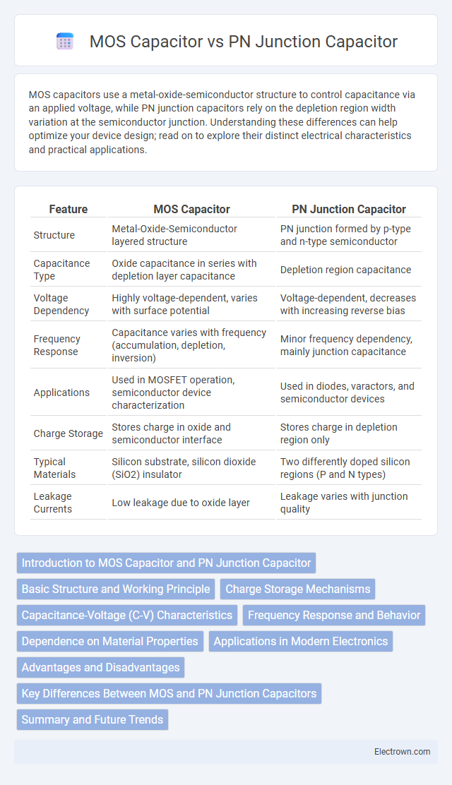
| Feature | MOS Capacitor | PN Junction Capacitor |
|---|---|---|
| Structure | Metal-Oxide-Semiconductor layered structure | PN junction formed by p-type and n-type semiconductor |
| Capacitance Type | Oxide capacitance in series with depletion layer capacitance | Depletion region capacitance |
| Voltage Dependency | Highly voltage-dependent, varies with surface potential | Voltage-dependent, decreases with increasing reverse bias |
| Frequency Response | Capacitance varies with frequency (accumulation, depletion, inversion) | Minor frequency dependency, mainly junction capacitance |
| Applications | Used in MOSFET operation, semiconductor device characterization | Used in diodes, varactors, and semiconductor devices |
| Charge Storage | Stores charge in oxide and semiconductor interface | Stores charge in depletion region only |
| Typical Materials | Silicon substrate, silicon dioxide (SiO2) insulator | Two differently doped silicon regions (P and N types) |
| Leakage Currents | Low leakage due to oxide layer | Leakage varies with junction quality |
Introduction to MOS Capacitor and PN Junction Capacitor
MOS capacitors consist of a metal-oxide-semiconductor structure that creates a controllable capacitance by varying the voltage applied across the metal gate and semiconductor. PN junction capacitors are formed by the depletion region at the interface of p-type and n-type semiconductor materials, where capacitance depends on the width of the depletion layer. Both devices are fundamental in semiconductor technology, with MOS capacitors widely used in MOSFET devices and PN junction capacitors critical in diodes and photodetectors.
Basic Structure and Working Principle
MOS capacitors consist of a metal gate, an oxide insulating layer, and a semiconductor substrate, creating a structure that modulates capacitance through accumulation, depletion, and inversion layers. PN junction capacitors form at the interface of p-type and n-type semiconductors, where the depletion region acts as a variable capacitor controlled by the reverse bias voltage. Your understanding of these devices benefits from recognizing that MOS capacitors rely on oxide capacitance and surface charge, while PN junction capacitors depend on the space-charge region width for their capacitance behavior.
Charge Storage Mechanisms
MOS capacitors store charge primarily through the formation of an inversion layer at the semiconductor-oxide interface, controlled by an applied voltage that modulates surface potential and electric field within the oxide layer. PN junction capacitors store charge via the depletion region, where the width of the depletion zone varies with the applied reverse-bias voltage, affecting the capacitance. Your device performance depends significantly on these distinct charge storage mechanisms, impacting capacitance-voltage characteristics and frequency response.
Capacitance-Voltage (C-V) Characteristics
MOS capacitors exhibit a distinct C-V characteristic featuring accumulation, depletion, and inversion regions, enabling precise control of surface potential via gate voltage modulation. In contrast, PN junction capacitors display a C-V curve primarily influenced by the depletion region width, which varies with reverse bias voltage, leading to non-linear capacitance changes. The MOS capacitor's ability to maintain a relatively constant oxide capacitance in accumulation contrasts with the PN junction capacitance that significantly decreases with increasing reverse bias due to widening depletion layer.
Frequency Response and Behavior
MOS capacitors exhibit a strong frequency-dependent behavior due to the formation of accumulation, depletion, and inversion layers, significantly affecting capacitance values at low, medium, and high frequencies. PN junction capacitors display a relatively stable capacitance with frequency, primarily governed by the depletion region width, which changes with applied voltage but shows minimal variation with frequency. The high-frequency response of MOS capacitors is limited by the slow generation and recombination of minority carriers, while PN junction capacitors maintain consistent capacitive characteristics due to majority carrier involvement.
Dependence on Material Properties
The MOS capacitor's capacitance strongly depends on the dielectric constant of the insulating oxide layer and the semiconductor substrate's doping concentration, influencing its charge storage and voltage response. In contrast, the PN junction capacitor's capacitance varies primarily with the depletion region width, which is determined by the semiconductor material's doping levels and intrinsic carrier concentration. Understanding these material property dependencies enables you to select the appropriate capacitor type for precise charge control and frequency response in your electronic designs.
Applications in Modern Electronics
MOS capacitors are integral in modern electronics for applications such as MOSFET gate capacitance, non-volatile memory cells, and advanced sensors due to their ability to modulate charge carriers at the oxide-semiconductor interface. PN junction capacitors find primary use in diode-based circuits, voltage regulation, and radio frequency tuning, leveraging their depletion region properties for charge storage and voltage responsiveness. Your choice between MOS and PN junction capacitors will depend on the specific electronic function, with MOS capacitors favored in integrated circuit design and PN junction capacitors common in discrete component applications.
Advantages and Disadvantages
MOS capacitors offer high capacitance density and excellent charge modulation capabilities, making them ideal for integrated circuit applications. However, they suffer from interface trap states and threshold voltage instability, which can affect reliability. PN junction capacitors provide stable capacitance with low leakage current and simplicity in fabrication, yet they exhibit limited capacitance tunability and are less suitable for high-frequency applications compared to MOS capacitors.
Key Differences Between MOS and PN Junction Capacitors
MOS capacitors feature a metal-oxide-semiconductor structure that allows variable capacitance controlled by gate voltage, enabling efficient modulation of charge storage. PN junction capacitors rely on the depletion region between p-type and n-type semiconductors, exhibiting capacitance that changes with applied reverse bias voltage but lacks the same level of control as MOS capacitors. Understanding these key differences helps you select the appropriate capacitor type for specific electronic applications, especially in integrated circuit design.
Summary and Future Trends
MOS capacitors exhibit high capacitance density and excellent scalability, making them essential in advanced semiconductor devices, while PN junction capacitors offer reliable depletion-region capacitance with low leakage currents. Ongoing research aims to enhance MOS capacitor performance through high-k dielectrics and 2D materials, whereas PN junction capacitors benefit from innovations in doping profiles and heterojunction engineering. Future trends point toward hybrid capacitor structures integrating MOS and PN junction characteristics to optimize speed, capacitance, and power efficiency in next-generation electronics.
MOS capacitor vs PN junction capacitor Infographic