RC delay measures the time taken for a signal to propagate through a resistive-capacitive network, significantly affecting the overall speed of integrated circuits, while gate delay refers to the intrinsic time a logic gate requires to switch its output after an input change. Understanding the distinction between these delays helps optimize Your circuit design for better performance and power efficiency--read on to explore how these factors influence electronic device speed.
Table of Comparison
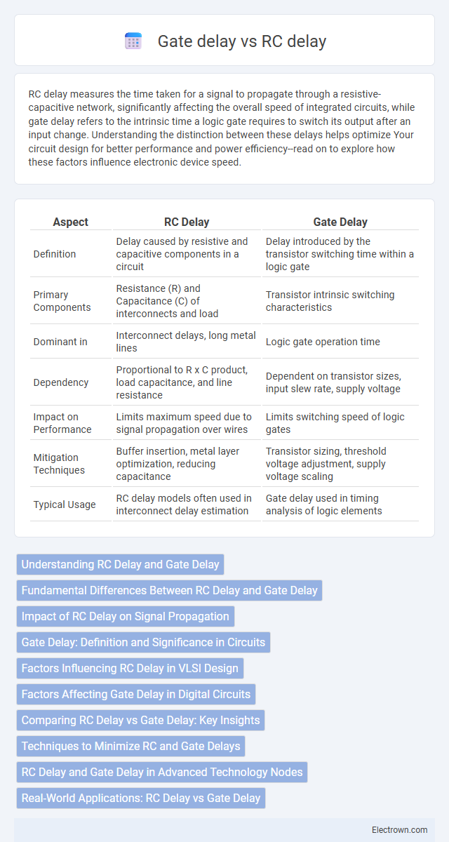
| Aspect | RC Delay | Gate Delay |
|---|---|---|
| Definition | Delay caused by resistive and capacitive components in a circuit | Delay introduced by the transistor switching time within a logic gate |
| Primary Components | Resistance (R) and Capacitance (C) of interconnects and load | Transistor intrinsic switching characteristics |
| Dominant in | Interconnect delays, long metal lines | Logic gate operation time |
| Dependency | Proportional to R x C product, load capacitance, and line resistance | Dependent on transistor sizes, input slew rate, supply voltage |
| Impact on Performance | Limits maximum speed due to signal propagation over wires | Limits switching speed of logic gates |
| Mitigation Techniques | Buffer insertion, metal layer optimization, reducing capacitance | Transistor sizing, threshold voltage adjustment, supply voltage scaling |
| Typical Usage | RC delay models often used in interconnect delay estimation | Gate delay used in timing analysis of logic elements |
Understanding RC Delay and Gate Delay
RC delay refers to the time delay caused by the resistance (R) and capacitance (C) in interconnects, impacting signal propagation speed in integrated circuits. Gate delay is the intrinsic time taken by a logic gate to switch states, influenced by its transistor characteristics and load capacitance. Understanding these delays helps optimize your circuit performance by balancing interconnect resistance-capacitance effects with gate switching speeds.
Fundamental Differences Between RC Delay and Gate Delay
RC delay arises from the resistance and capacitance in the interconnects, impacting the signal propagation time through the wiring between gates. Gate delay is intrinsic to the logic gate itself, determined by the transistor switching characteristics and loading within the gate. Understanding these fundamental differences allows you to optimize circuit timing by addressing both interconnect parasitics and gate performance separately.
Impact of RC Delay on Signal Propagation
RC delay significantly affects signal propagation by increasing the time it takes for a signal to travel through a circuit due to resistance (R) and capacitance (C) within interconnects. This delay limits the maximum operating frequency and overall speed of digital circuits, causing timing bottlenecks in high-speed designs. Understanding and minimizing RC delay is crucial for optimizing Your circuit performance and ensuring reliable signal transmission.
Gate Delay: Definition and Significance in Circuits
Gate delay refers to the time it takes for a digital logic gate to respond to an input change and produce the corresponding output. This delay is critical in determining the overall speed and performance of digital circuits, as it directly affects signal propagation and timing accuracy. Understanding and minimizing gate delay enables more efficient circuit design, improving reliability and operational frequency.
Factors Influencing RC Delay in VLSI Design
RC delay in VLSI design is primarily influenced by the resistance and capacitance of interconnects, which depend on factors like wire length, width, material conductivity, and the dielectric constant of the insulating layer. As technology nodes shrink, increased interconnect density and reduced cross-sectional area raise resistance, while proximity to neighboring wires increases parasitic capacitance, both exacerbating RC delay. Managing these parameters is crucial for optimizing overall circuit performance and minimizing signal propagation delay beyond intrinsic gate delay.
Factors Affecting Gate Delay in Digital Circuits
Gate delay in digital circuits is primarily influenced by load capacitance, supply voltage, and transistor sizing, with larger capacitance increasing the time required to charge or discharge the gate node. Process variations, temperature fluctuations, and threshold voltage also contribute to delay variability by affecting transistor switching speed. Minimizing RC delay through optimized interconnect design complements gate delay reduction, enhancing overall circuit performance.
Comparing RC Delay vs Gate Delay: Key Insights
RC delay arises from the resistance-capacitance network within interconnects, significantly impacting signal propagation speed as wire lengths increase. Gate delay depends on the intrinsic switching time of transistors within logic gates, influenced by device size and input loading. Understanding the balance between RC delay and gate delay is crucial for optimizing your circuit's timing and overall performance in advanced integrated circuits.
Techniques to Minimize RC and Gate Delays
Techniques to minimize RC delay include reducing parasitic capacitance through optimized layout design, using low-resistance interconnect materials like copper, and implementing buffering strategies such as inserting repeaters to shorten wire length segments. Gate delay reduction is achieved by transistor sizing optimization to balance drive strength with load capacitance, utilizing high-threshold voltage devices selectively, and applying advanced CMOS technologies featuring faster switching speeds. Combining these approaches enables efficient timing performance by addressing both the resistive-capacitive delay and intrinsic gate switching characteristics in integrated circuits.
RC Delay and Gate Delay in Advanced Technology Nodes
RC delay in advanced technology nodes results from increased interconnect resistance and capacitance, significantly impacting signal integrity and timing reliability. Gate delay, influenced by transistor switching speed and intrinsic capacitances, remains critical but often becomes overshadowed by RC delay in deep submicron processes. Your chip design must balance these delays by optimizing both device-level performance and interconnect engineering to ensure optimal circuit speed.
Real-World Applications: RC Delay vs Gate Delay
RC delay and gate delay critically impact the timing and performance of integrated circuits in real-world applications such as high-speed processors and memory devices. RC delay, caused by resistive and capacitive interconnects, dominates signal propagation time in long metal lines, affecting clock distribution and data integrity. Your circuit design must balance and minimize both RC and gate delays to optimize speed, power consumption, and overall system reliability.
RC delay vs gate delay Infographic