Source follower and emitter follower are both voltage buffer configurations used in analog circuits, with the source follower operating in MOSFET transistors and the emitter follower using BJTs, each providing high input impedance and low output impedance for signal buffering. Explore the rest of the article to understand the key differences and practical applications of these two essential amplifier stages for your electronic projects.
Table of Comparison
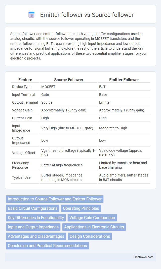
| Feature | Source Follower | Emitter Follower |
|---|---|---|
| Device Type | MOSFET | BJT |
| Input Terminal | Gate | Base |
| Output Terminal | Source | Emitter |
| Voltage Gain | Approximately 1 (unity gain) | Approximately 1 (unity gain) |
| Current Gain | High | High |
| Input Impedance | Very High (due to MOSFET gate) | Moderate to High |
| Output Impedance | Low | Low |
| Voltage Offset | Vgs threshold voltage (typically 1-3 V) | Vbe diode voltage (approx. 0.6-0.7 V) |
| Frequency Response | Better at high frequencies | Limited by transistor beta and base charging |
| Typical Use | Buffer stages, impedance matching in MOS circuits | Audio amplifiers, buffer stages in BJT circuits |
Introduction to Source Follower and Emitter Follower
Source followers and emitter followers are fundamental voltage buffer configurations used in electronic circuits to provide high input impedance and low output impedance. The source follower, based on a MOSFET, allows for unity voltage gain with high input impedance, making it ideal for impedance matching in analog circuits. In contrast, the emitter follower employs a bipolar junction transistor (BJT) to achieve similar buffering characteristics, emphasizing low output impedance for driving loads effectively while maintaining signal integrity.
Basic Circuit Configurations
Source followers utilize an n-channel MOSFET with the input signal applied to the gate, the source serving as the output, and the drain connected to a constant voltage supply, providing high input impedance and low output impedance. Emitter followers employ an NPN bipolar junction transistor (BJT) where the input is fed into the base, the emitter provides the output, and the collector is connected to a power supply, offering current gain and voltage buffering. Both configurations are voltage buffer stages, but the source follower is preferred in MOSFET designs for its simpler biasing and input characteristics, whereas the emitter follower is common in BJTs for its linear operation and simple fixed biasing.
Operating Principles
A source follower operates by using a MOSFET where the output voltage closely follows the input voltage minus a small threshold voltage, providing high input impedance and low output impedance ideal for voltage buffering. An emitter follower uses a bipolar junction transistor (BJT) where the output voltage is approximately the input voltage minus the base-emitter voltage drop, delivering similar buffering characteristics with a slightly lower input impedance compared to source followers. Your choice between the two depends on the specific transistor characteristics and the desired impedance and voltage gain requirements in your circuit design.
Key Differences in Functionality
A source follower operates as a voltage buffer using a MOSFET with its output at the source terminal, providing high input impedance and low output impedance ideal for impedance matching. An emitter follower uses a bipolar junction transistor (BJT) with its output at the emitter, offering similar buffering characteristics but with lower input impedance compared to the source follower. Key differences in functionality arise from their transistor types, impacting voltage gain, input/output impedance, and frequency response in analog circuit applications.
Voltage Gain Comparison
Source followers and emitter followers both exhibit voltage gains slightly less than unity, typically around 0.9 to 0.98, due to their inherent transistor characteristics. The emitter follower, using a bipolar junction transistor (BJT), generally achieves a voltage gain closer to unity because of its high input impedance and low output impedance, minimizing signal loss. In contrast, the source follower, based on a field-effect transistor (FET), may display marginally lower voltage gain influenced by the device's transconductance and channel resistance, affecting its efficiency in voltage buffering applications.
Input and Output Impedance
A source follower typically exhibits high input impedance and low output impedance, making it ideal for impedance matching in voltage buffer applications. An emitter follower also provides high input impedance and low output impedance, but generally has a lower input impedance compared to a source follower due to the base-emitter junction characteristics. Both configurations are used to achieve voltage buffering, but the source follower often offers better isolation and less loading on the preceding stage due to its higher input impedance.
Applications in Electronic Circuits
Source followers are widely used in analog circuits for impedance matching due to their high input impedance and low output impedance, making them ideal as voltage buffers in RF and audio applications. Emitter followers serve a similar buffering function in transistor circuits, providing current gain with minimal voltage drop, frequently applied in amplifier output stages and switching circuits. Both configurations enhance signal stability and drive capability while preventing loading effects in cascaded amplifier stages.
Advantages and Disadvantages
Source follower circuits offer high input impedance and low output impedance, making them ideal for buffering and impedance matching in MOSFET applications, but they exhibit a voltage drop close to the threshold voltage, which can limit voltage swing. Emitter followers provide low output impedance and unity voltage gain with excellent linearity in BJTs, yet they consume more power due to transistor bias current and have a voltage drop of approximately 0.7V across the junction. When choosing between these configurations, consider the trade-offs between voltage headroom, power consumption, and signal buffering needs to optimize Your circuit's performance.
Design Considerations
Source follower and emitter follower circuits both offer voltage buffering with high input impedance and low output impedance, but design considerations differ significantly due to transistor type and biasing requirements. In source followers using MOSFETs, careful threshold voltage and gate-source voltage control are crucial to maintain linear operation, while emitter followers with BJTs demand precise base current biasing to ensure proper transistor conduction and stability. Your choice depends on power supply constraints, frequency response, and integration compatibility, with MOSFET source followers typically favored in low-voltage digital applications and emitter followers preferred in analog linear amplification.
Conclusion and Practical Recommendations
Source followers and emitter followers both serve as voltage buffers with high input impedance and low output impedance, yet source followers based on MOSFETs offer better thermal stability and lower distortion compared to emitter followers using BJTs. Your choice depends on the specific application requirements: use source followers for low-noise, high-impedance input stages and emitter followers when wider bandwidth and higher gain linearity are prioritized. For practical circuit design, consider the power supply constraints, device availability, and desired frequency response when selecting between these two follower configurations.
Source follower vs emitter follower Infographic