Charge injection occurs when a MOSFET switch changes state, causing a small amount of charge to be transferred unintentionally to the output node, while clock feedthrough results from capacitive coupling between the clock signal and the output, leading to unwanted voltage spikes. Understanding these phenomena is crucial for minimizing signal distortion in switched-capacitor circuits; explore the rest of this article to learn how you can effectively reduce their impact.
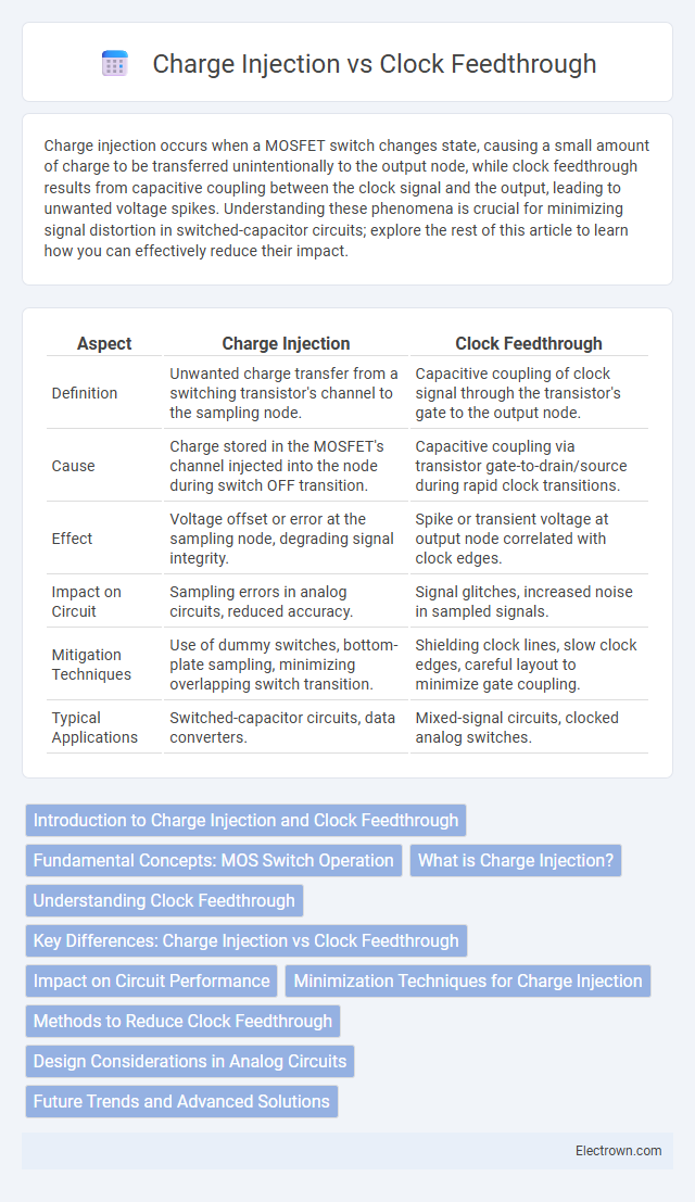
Table of Comparison
| Aspect | Charge Injection | Clock Feedthrough |
|---|---|---|
| Definition | Unwanted charge transfer from a switching transistor's channel to the sampling node. | Capacitive coupling of clock signal through the transistor's gate to the output node. |
| Cause | Charge stored in the MOSFET's channel injected into the node during switch OFF transition. | Capacitive coupling via transistor gate-to-drain/source during rapid clock transitions. |
| Effect | Voltage offset or error at the sampling node, degrading signal integrity. | Spike or transient voltage at output node correlated with clock edges. |
| Impact on Circuit | Sampling errors in analog circuits, reduced accuracy. | Signal glitches, increased noise in sampled signals. |
| Mitigation Techniques | Use of dummy switches, bottom-plate sampling, minimizing overlapping switch transition. | Shielding clock lines, slow clock edges, careful layout to minimize gate coupling. |
| Typical Applications | Switched-capacitor circuits, data converters. | Mixed-signal circuits, clocked analog switches. |
Introduction to Charge Injection and Clock Feedthrough
Charge injection occurs when a switching transistor injects charge into the switched node, causing voltage errors in analog circuits. Clock feedthrough is the unintended coupling of the clock signal through parasitic capacitances into the output node, resulting in signal distortion and timing issues. Both phenomena significantly impact the accuracy and performance of switched-capacitor circuits and sample-and-hold amplifiers.
Fundamental Concepts: MOS Switch Operation
Charge injection and clock feedthrough are critical phenomena affecting MOS switch operation in analog circuits. Charge injection occurs when the MOS switch transitions between on and off states, causing channel charge to transfer to the output node, resulting in voltage glitches. Clock feedthrough arises from capacitive coupling between the gate and channel, transmitting clock signal variations directly to the output, which can degrade signal integrity.
What is Charge Injection?
Charge injection occurs when a MOSFET switch transitions from the on to the off state, causing a redistribution of charge from the gate channel into the substrate or the output node. This unwanted transfer can introduce voltage glitches and degrade signal integrity in precision analog circuits like sample-and-hold amplifiers. Understanding your circuit's charge injection characteristics is crucial for minimizing errors and ensuring accurate signal processing.
Understanding Clock Feedthrough
Clock feedthrough occurs when the switching of a clock signal couples unwanted charge into a sensitive node, causing voltage glitches that can degrade circuit performance. This phenomenon primarily results from capacitive coupling between the clock line and the signal path, leading to unintended signal distortion. Understanding clock feedthrough helps you minimize timing errors and improve the accuracy of analog and mixed-signal integrated circuits.
Key Differences: Charge Injection vs Clock Feedthrough
Charge injection occurs when the MOSFET switch's channel charge is transferred to the output node during switching, causing a voltage glitch proportional to the gate capacitance and charge density. Clock feedthrough, on the other hand, results from capacitive coupling between the clock signal and output node through the gate-to-channel overlap capacitance, producing an undesired voltage spike correlated with clock amplitude and frequency. Charge injection is primarily influenced by transistor size and oxide thickness, while clock feedthrough depends on device parasitic capacitances and clock signal characteristics.
Impact on Circuit Performance
Charge injection causes unwanted voltage spikes at the output node of a switched capacitor circuit, leading to signal distortion and reduced accuracy. Clock feedthrough introduces parasitic coupling of the clock signal into the sensitive nodes, generating noise that degrades the circuit's signal-to-noise ratio and overall stability. Minimizing these effects is crucial for maintaining the integrity and precision of your analog and mixed-signal circuit performance.
Minimization Techniques for Charge Injection
Minimization techniques for charge injection primarily involve optimizing switch design by using complementary switches and minimizing overlap between control signals and the channel conduction state. Implementing dummy switches or using transmission gates helps balance and cancel injected charge, significantly reducing signal distortion in switched capacitor circuits. Careful timing control and layout strategies further suppress charge injection effects, enhancing overall analog signal integrity.
Methods to Reduce Clock Feedthrough
To reduce clock feedthrough in integrated circuits, careful layout design techniques such as increasing the distance between clock lines and sensitive nodes are essential. The use of complementary switches and adjusting transistor sizes helps minimize capacitive coupling effect. Shielding clock lines with grounded guard rings further isolates signal paths, protecting your circuit from unwanted charge injection.
Design Considerations in Analog Circuits
Charge injection and clock feedthrough critically impact precision in analog circuit design, requiring careful transistor sizing and switch timing to minimize errors. Optimizing switch architecture and employing complementary switches can reduce charge injection effects, while layout strategies and shielding guard against clock feedthrough noise. Accurate modeling of these phenomena during simulation ensures improved signal integrity and reliable performance in sampled-data systems.
Future Trends and Advanced Solutions
Emerging semiconductor technologies prioritize minimizing charge injection and clock feedthrough through advanced transistor designs and novel insulating materials that enhance signal integrity in high-speed circuits. Machine learning algorithms are increasingly utilized to predict and compensate for these parasitic effects, enabling more precise analog and mixed-signal system performance. Future solutions also explore adaptive calibration techniques in real-time to dynamically counteract charge injection and clock feedthrough, optimizing low-power applications in IoT and wearable devices.
Charge injection vs clock feedthrough Infographic