Schematic driven design prioritizes the creation of a detailed circuit diagram before translating it into physical layout, ensuring logical accuracy and functionality early in the process. Understanding the differences between schematic driven and layout driven design can help you optimize your workflow and improve your project outcomes; explore the rest of this article to learn more.
Table of Comparison
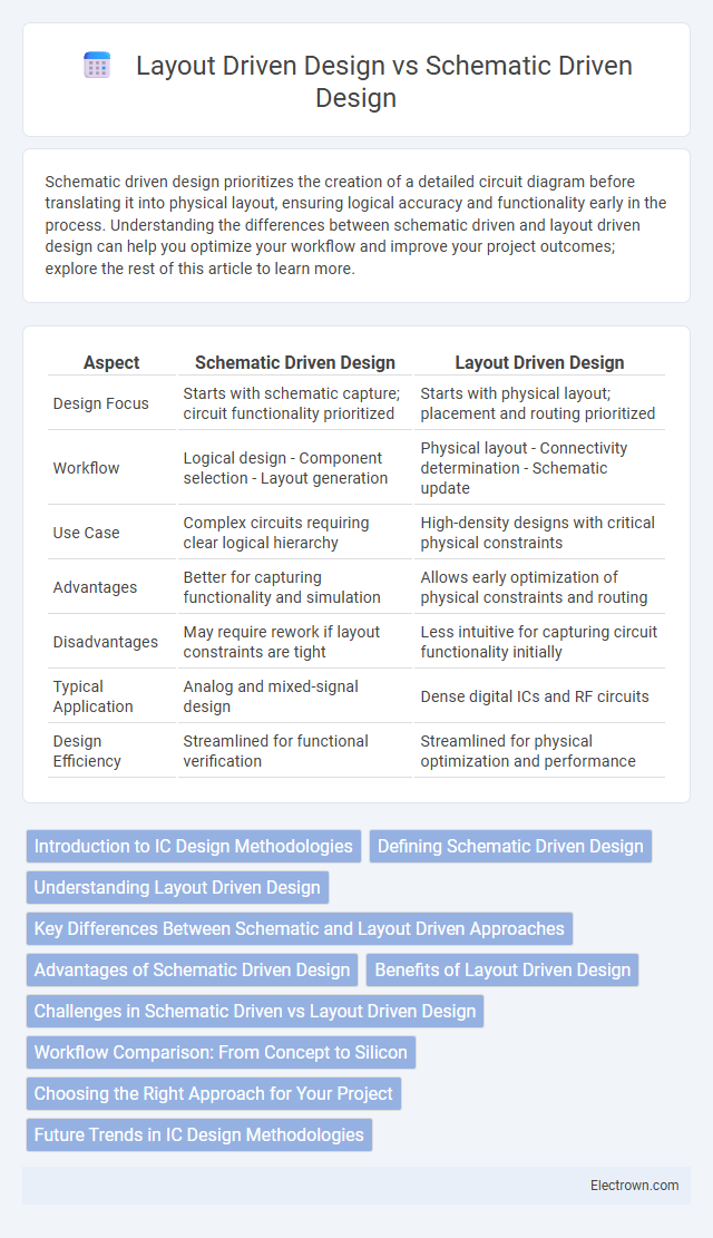
| Aspect | Schematic Driven Design | Layout Driven Design |
|---|---|---|
| Design Focus | Starts with schematic capture; circuit functionality prioritized | Starts with physical layout; placement and routing prioritized |
| Workflow | Logical design - Component selection - Layout generation | Physical layout - Connectivity determination - Schematic update |
| Use Case | Complex circuits requiring clear logical hierarchy | High-density designs with critical physical constraints |
| Advantages | Better for capturing functionality and simulation | Allows early optimization of physical constraints and routing |
| Disadvantages | May require rework if layout constraints are tight | Less intuitive for capturing circuit functionality initially |
| Typical Application | Analog and mixed-signal design | Dense digital ICs and RF circuits |
| Design Efficiency | Streamlined for functional verification | Streamlined for physical optimization and performance |
Introduction to IC Design Methodologies
Schematic driven design emphasizes creating and verifying circuit functionality through symbolic representation before physical layout, ensuring logical correctness early in the integrated circuit (IC) development process. Layout driven design focuses on physical placement and routing within the IC, prioritizing geometric constraints, device dimensions, and parasitics to optimize performance and manufacturability. Understanding these methodologies enables you to balance design accuracy and efficiency in complex IC projects.
Defining Schematic Driven Design
Schematic Driven Design is a methodology in electronic design automation where the circuit's functionality and connectivity are defined first through detailed schematic diagrams before progressing to the physical layout stage. This approach emphasizes accurate electrical representation and logical correctness, ensuring that the design intent is preserved throughout the development process. By prioritizing schematic creation, designers can detect and resolve errors early, improving the reliability and efficiency of the final integrated circuit or printed circuit board design.
Understanding Layout Driven Design
Layout Driven Design emphasizes designing the physical placement of circuit components on a chip or PCB before finalizing the schematic, enabling better optimization of space, signal integrity, and routing paths. This approach benefits complex designs by allowing engineers to address timing issues and manufacturability constraints early in the layout phase, improving overall performance. You gain increased control over physical parameters, ensuring the final product meets strict design specifications and industry standards.
Key Differences Between Schematic and Layout Driven Approaches
Schematic driven design prioritizes the creation of a complete circuit schematic before any layout work begins, ensuring accurate electrical connectivity and functionality. Layout driven design starts with the physical placement and routing, allowing designers to modify the schematic dynamically based on real-time layout constraints. Key differences include the sequencing of design steps, with schematic driven focusing on electrical correctness first, while layout driven emphasizes physical optimization and iterative refinement.
Advantages of Schematic Driven Design
Schematic driven design offers enhanced accuracy in circuit functionality verification through early simulation and validation, reducing design errors before layout implementation. This approach simplifies modification processes since changes in the schematic automatically propagate to the layout, increasing efficiency and consistency. Furthermore, it enables better collaboration among design teams by providing a clear and structured representation of the electrical connections and component relationships.
Benefits of Layout Driven Design
Layout Driven Design improves design accuracy by allowing real-time physical constraints and geometries to guide the development process, reducing errors between schematic and physical implementation. This approach enhances manufacturing quality by integrating design with physical fabrication rules early, optimizing for yield and reliability. It accelerates time-to-market as modifications in layout reflect immediately in the design, streamlining verification and minimizing rework cycles.
Challenges in Schematic Driven vs Layout Driven Design
Schematic Driven Design often faces challenges in maintaining accurate synchronization between the schematic and layout, which can lead to errors during the physical implementation phase. Layout Driven Design encounters difficulties in integrating complex circuit topology changes without disrupting the manual placement and routing efforts already committed. Both design methodologies struggle with ensuring design rule compliance and timing closure, but Schematic Driven Design typically requires more intensive verification due to its reliance on abstract representations.
Workflow Comparison: From Concept to Silicon
Schematic-driven design initiates the workflow with a detailed circuit schematic, ensuring precise logical functionality before transitioning to physical layout, optimizing early-stage verification and reducing iteration cycles. Layout-driven design starts with the physical placement and routing, allowing designers to address spatial constraints and physical effects upfront, which is beneficial for complex analog or mixed-signal circuits requiring close component coupling. The contrast in workflows influences design iteration speed, error mitigation, and integration efficiency, with schematic-driven emphasizing logical correctness first and layout-driven prioritizing physical feasibility from concept to silicon realization.
Choosing the Right Approach for Your Project
Schematic driven design emphasizes creating a detailed circuit schematic first, ensuring precise functionality before moving to layout, which optimizes signal integrity and design accuracy. Layout driven design starts with the physical board layout, enabling you to focus on component placement and routing constraints early, valuable for complex or space-constrained projects. Understanding your project's priorities--whether functional validation or spatial optimization--is critical to selecting the best approach for efficient and effective PCB design.
Future Trends in IC Design Methodologies
Future trends in IC design methodologies emphasize integrating AI-driven tools and machine learning algorithms to enhance both schematic and layout-driven design processes, enabling faster iteration and improved accuracy. The rise of heterogeneous integration and 3D ICs demands more sophisticated co-optimization between schematics and layouts, ensuring better performance and reduced power consumption. Adopting these advanced methodologies will empower your design workflow to manage complexity and meet the stringent requirements of next-generation semiconductor technologies.
Schematic Driven vs Layout Driven Design Infographic