Gate oxide acts as a thin insulating layer crucial for controlling the flow of electrons in a MOSFET transistor, while field oxide serves as a thicker layer that isolates different regions of a semiconductor device to prevent electrical interference. Understanding the distinct roles and characteristics of these oxides is essential for optimizing semiconductor device performance; continue reading to explore their applications and differences in detail.
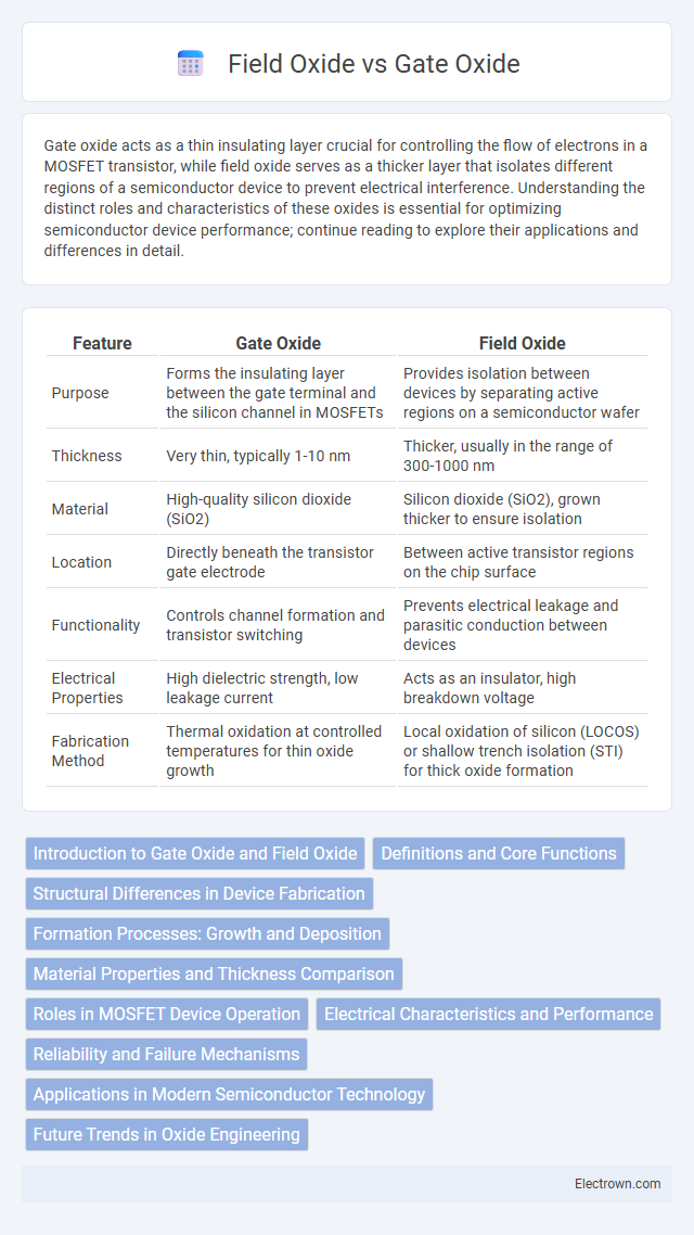
Table of Comparison
| Feature | Gate Oxide | Field Oxide |
|---|---|---|
| Purpose | Forms the insulating layer between the gate terminal and the silicon channel in MOSFETs | Provides isolation between devices by separating active regions on a semiconductor wafer |
| Thickness | Very thin, typically 1-10 nm | Thicker, usually in the range of 300-1000 nm |
| Material | High-quality silicon dioxide (SiO2) | Silicon dioxide (SiO2), grown thicker to ensure isolation |
| Location | Directly beneath the transistor gate electrode | Between active transistor regions on the chip surface |
| Functionality | Controls channel formation and transistor switching | Prevents electrical leakage and parasitic conduction between devices |
| Electrical Properties | High dielectric strength, low leakage current | Acts as an insulator, high breakdown voltage |
| Fabrication Method | Thermal oxidation at controlled temperatures for thin oxide growth | Local oxidation of silicon (LOCOS) or shallow trench isolation (STI) for thick oxide formation |
Introduction to Gate Oxide and Field Oxide
Gate oxide, a thin insulating layer of silicon dioxide, is crucial in MOSFET devices to separate the gate terminal from the underlying silicon channel, enabling effective control of the transistor's switching behavior. Field oxide, on the other hand, is a thicker oxide layer used to isolate different components on a semiconductor wafer, preventing electrical interference and leakage between adjacent devices. Your understanding of these oxides is essential for optimizing semiconductor device performance and reliability.
Definitions and Core Functions
Gate oxide is a thin insulating layer of silicon dioxide located between the transistor gate and the underlying silicon substrate, enabling precise control of current flow in MOSFET devices. Field oxide, in contrast, is a much thicker oxide layer used to isolate different transistors on a silicon wafer and prevent electrical crosstalk and leakage. Understanding these core functions helps you optimize device reliability and performance in semiconductor manufacturing.
Structural Differences in Device Fabrication
Gate oxide is a thin, uniform layer of silicon dioxide deposited directly on the silicon substrate, serving as the critical insulating barrier in MOSFETs that controls the channel formation. Field oxide, in contrast, is a much thicker oxide layer grown through the LOCOS process or deposited via STI techniques, used primarily for device isolation and preventing leakage currents between adjacent transistors. The structural difference lies in the gate oxide's nanoscale thickness enabling precise gate control, while field oxide's microscale thickness provides robust electrical isolation in integrated circuits.
Formation Processes: Growth and Deposition
Gate oxide is typically grown using thermal oxidation, where silicon wafers are exposed to oxygen or steam at high temperatures to form a thin, uniform silicon dioxide layer crucial for transistor gate insulators. Field oxide is generally formed by a local oxidation of silicon (LOCOS) process, involving masking regions with silicon nitride before thermal oxidation to grow thicker oxide areas for device isolation. Unlike deposited oxides that use chemical vapor deposition (CVD) to apply oxide layers, gate and field oxides rely primarily on controlled thermal growth to ensure superior interface quality and electrical characteristics.
Material Properties and Thickness Comparison
Gate oxide, typically silicon dioxide (SiO2), is much thinner, around 1-10 nm, providing excellent dielectric properties for strong gate control and minimal leakage in MOSFET devices. Field oxide, also silicon dioxide but grown thicker at 100-1000 nm, acts as an insulating layer to isolate device components and reduce parasitic capacitance. Your device's performance depends on the precise control of these oxide thicknesses and their uniform material quality to ensure reliability and electrical characteristics.
Roles in MOSFET Device Operation
Gate oxide in a MOSFET acts as a crucial insulating layer that enables gate control over the channel by separating the gate electrode from the semiconductor substrate, allowing the electric field to modulate current flow. Field oxide, on the other hand, provides isolation between devices by preventing leakage currents and electrical interference in adjacent regions, ensuring device stability and preventing short circuits. Understanding the specific role of each oxide layer helps optimize Your MOSFET's performance, reliability, and scaling in integrated circuits.
Electrical Characteristics and Performance
Gate oxide exhibits a high dielectric constant and thin thickness, enabling superior gate control and faster transistor switching speeds due to reduced capacitance and leakage currents. Field oxide, significantly thicker with lower dielectric strength, serves primarily as insulation to prevent current leakage between devices, enhancing overall chip reliability but limiting electrical conduction. Your device's performance depends on optimizing gate oxide thickness for speed while using field oxide to manage parasitic effects and electrical isolation.
Reliability and Failure Mechanisms
Gate oxide exhibits higher susceptibility to time-dependent dielectric breakdown (TDDB) due to its ultra-thin thickness, making reliability a critical concern in advanced CMOS technologies. Field oxide, being thicker and used for isolation, primarily encounters issues related to stress-induced leakage current (SILC) and limited susceptibility to oxide charge trapping. Understanding the distinct failure mechanisms in gate oxide, such as hot carrier injection and bias temperature instability, versus the more stable behavior of field oxide, is essential for optimizing device longevity and performance.
Applications in Modern Semiconductor Technology
Gate oxide serves as the critical insulating layer in MOSFET transistors, enabling precise control of channel conductivity and enhancing device switching performance in modern integrated circuits. Field oxide, meanwhile, acts as an isolation layer, preventing electrical interference between adjacent components and ensuring circuit reliability in complex semiconductor layouts. Both oxides are essential in advanced CMOS technology, supporting high-density integration and low power consumption in processors, memory chips, and microcontrollers.
Future Trends in Oxide Engineering
Future trends in oxide engineering emphasize the development of ultra-thin gate oxides with high-k dielectric materials to enhance transistor performance and reduce leakage currents in advanced CMOS technologies. Field oxide engineering is progressing towards shallow trench isolation (STI) techniques that minimize parasitic capacitance and improve device scaling. Integration of novel materials like hafnium oxide and advanced patterning methods are critical for optimizing both gate oxide and field oxide characteristics in next-generation semiconductor devices.
Gate Oxide vs Field Oxide Infographic