TSV (Through-Silicon Via) offers lower resistance and inductance compared to traditional wire bonding, enabling faster signal transmission and better performance in 3D integrated circuits. Discover how these advanced packaging technologies impact your device design and functionality by reading the rest of the article.
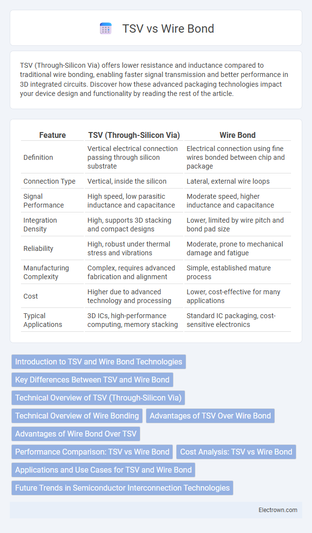
Table of Comparison
| Feature | TSV (Through-Silicon Via) | Wire Bond |
|---|---|---|
| Definition | Vertical electrical connection passing through silicon substrate | Electrical connection using fine wires bonded between chip and package |
| Connection Type | Vertical, inside the silicon | Lateral, external wire loops |
| Signal Performance | High speed, low parasitic inductance and capacitance | Moderate speed, higher inductance and capacitance |
| Integration Density | High, supports 3D stacking and compact designs | Lower, limited by wire pitch and bond pad size |
| Reliability | High, robust under thermal stress and vibrations | Moderate, prone to mechanical damage and fatigue |
| Manufacturing Complexity | Complex, requires advanced fabrication and alignment | Simple, established mature process |
| Cost | Higher due to advanced technology and processing | Lower, cost-effective for many applications |
| Typical Applications | 3D ICs, high-performance computing, memory stacking | Standard IC packaging, cost-sensitive electronics |
Introduction to TSV and Wire Bond Technologies
Through-Silicon Via (TSV) technology enables vertical electrical connections by creating tiny, conductive vias through silicon wafers, enhancing performance in 3D integrated circuits. Wire bonding, a traditional packaging technique, uses fine metal wires to interconnect semiconductor devices with external leads, offering reliability and cost-effectiveness in 2D chip assembly. TSV provides superior signal integrity and reduced parasitics compared to wire bonds, making it ideal for high-density, high-speed applications.
Key Differences Between TSV and Wire Bond
Through-Silicon Via (TSV) technology enables vertical electrical connections directly through silicon wafers, offering shorter interconnect distances and improved signal performance compared to traditional Wire Bond methods. Wire Bonding uses fine metallic wires to connect semiconductor components to package leads, which can introduce longer signal paths and higher parasitic capacitance. TSV provides enhanced power efficiency, signal integrity, and higher density integration, making it ideal for advanced 3D IC packaging, whereas Wire Bond remains prevalent for cost-effective and simpler 2D packaging solutions.
Technical Overview of TSV (Through-Silicon Via)
Through-Silicon Via (TSV) technology enables vertical electrical connections passing directly through silicon wafers, significantly improving inter-chip communication and reducing signal delay compared to traditional wire bonding. TSVs offer higher bandwidth and lower power consumption by minimizing parasitic inductance and capacitance found in planar connections. This advanced 3D integration approach supports increased device density and enhanced performance in modern semiconductor packaging.
Technical Overview of Wire Bonding
Wire bonding is a microelectronic interconnection technique that uses fine metal wires, typically gold or aluminum, to create electrical connections between a semiconductor chip and its package substrate. This method offers high reliability and flexibility in complex circuit designs, featuring processes such as ball bonding and wedge bonding for precise and efficient assembly. Your choice between wire bonding and technologies like Through-Silicon Via (TSV) depends on factors like cost, performance requirements, and application complexity.
Advantages of TSV Over Wire Bond
Through-Silicon Via (TSV) technology offers significant advantages over traditional wire bonding, including higher interconnection density and reduced signal path length, which enhance electrical performance and enable faster data transmission. TSV also improves thermal management by providing better heat dissipation through vertical stacking, supporting more compact and efficient multi-chip modules. Your designs benefit from TSV's lower inductance and capacitance, leading to enhanced reliability and power efficiency in advanced semiconductor packaging.
Advantages of Wire Bond Over TSV
Wire bonding offers cost-effective manufacturing with simpler and more established processes compared to Through-Silicon Via (TSV) technology. It provides greater design flexibility for connecting chips with varying sizes and enables easier rework or repair during assembly. Wire bonding remains a reliable choice for lower-density interconnections and less complex 3D integration applications.
Performance Comparison: TSV vs Wire Bond
Through-Silicon Via (TSV) technology exhibits superior electrical performance compared to traditional Wire Bond techniques, primarily due to shorter interconnect lengths that reduce signal delay and parasitic capacitance. TSV enables higher bandwidth and lower power consumption in 3D integrated circuits, enhancing overall system efficiency and speed. Wire Bond, while cost-effective and well-established, faces limitations in scaling and signal integrity at high frequencies, making TSV the preferred choice for advanced semiconductor packaging.
Cost Analysis: TSV vs Wire Bond
Through-Silicon Via (TSV) technology generally involves higher upfront manufacturing costs due to complex fabrication processes and advanced equipment requirements compared to traditional Wire Bond techniques. Wire Bond offers a more cost-effective solution for lower to medium volume production with simpler assembly and testing, making it ideal for budget-sensitive projects. Your choice between TSV and Wire Bond should consider volume requirements, performance needs, and overall cost implications for a balanced cost analysis.
Applications and Use Cases for TSV and Wire Bond
TSV (Through-Silicon Via) technology is widely used in 3D integrated circuits and advanced packaging for high-performance computing, memory stacks, and mobile devices due to its ability to provide shorter interconnects and higher bandwidth. Wire bonding remains prevalent in cost-sensitive applications such as automotive electronics, power devices, and traditional semiconductor packaging where reliability and established manufacturing processes are critical. TSV is favored in applications requiring high-density integration and low latency, while wire bonding suits applications prioritizing simplicity and lower cost.
Future Trends in Semiconductor Interconnection Technologies
Through-Silicon Via (TSV) technology outpaces traditional wire bonding by enabling significantly higher interconnect density and reduced signal latency, critical for advanced 3D integrated circuits (ICs) and heterogeneous integration. Wire bonding, while cost-effective and reliable, faces limitations in scalability and frequency performance, making TSV the preferred choice for next-generation high-performance computing, AI accelerators, and memory stacking applications. Emerging trends point towards hybrid approaches combining TSV with micro-bumps and fine-pitch interposers to optimize bandwidth, power consumption, and thermal management in semiconductor packaging.
TSV vs Wire Bond Infographic