Charge trapping occurs when electrons or holes become localized at defects or interfaces, impeding charge flow and affecting device performance, while quantum confinement restricts electron movement within nanoscale dimensions, altering energy levels and optical properties. Understanding the differences between charge trapping and quantum confinement is essential for optimizing your semiconductor and nanodevice applications, so continue exploring the detailed comparisons in this article.
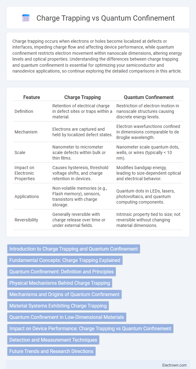
Table of Comparison
| Feature | Charge Trapping | Quantum Confinement |
|---|---|---|
| Definition | Retention of electrical charge in defect sites or traps within a material. | Restriction of electron motion in nanoscale structures causing discrete energy levels. |
| Mechanism | Electrons are captured and held by localized defect states. | Electron wavefunctions confined in dimensions comparable to de Broglie wavelength. |
| Scale | Nanometer to micrometer scale defects within bulk or thin films. | Nanometer scale quantum dots, wells, or wires (typically < 10 nm). |
| Impact on Electronic Properties | Causes hysteresis, threshold voltage shifts, and charge retention in devices. | Modifies bandgap energy, leading to size-dependent optical and electrical behavior. |
| Applications | Non-volatile memories (e.g., Flash memory), sensors, transistors with charge storage. | Quantum dots in LEDs, lasers, photovoltaics, and quantum computing components. |
| Reversibility | Generally reversible with charge release over time or under external fields. | Intrinsic property tied to size; not reversible without changing material dimensions. |
Introduction to Charge Trapping and Quantum Confinement
Charge trapping occurs when electrons or holes become localized at defect sites or interfaces within a material, affecting its electrical properties and device performance. Quantum confinement arises when the size of a semiconductor crystal is reduced to a scale comparable to the electron's de Broglie wavelength, leading to discrete energy levels and altered optical and electronic behaviors. Understanding how charge trapping influences your device's efficiency and how quantum confinement modifies carrier dynamics is crucial for optimizing nanoscale electronic and optoelectronic applications.
Fundamental Concepts: Charge Trapping Explained
Charge trapping refers to the phenomenon where charge carriers, such as electrons or holes, become localized in defect sites or energy states within a material, impacting electronic device performance. Quantum confinement occurs when the dimensions of a semiconductor are reduced to the nanoscale, altering its electronic and optical properties due to spatial restriction of charge carriers. Understanding charge trapping is crucial for optimizing your semiconductor devices, as it influences retention time, threshold voltage shifts, and overall reliability.
Quantum Confinement: Definition and Principles
Quantum confinement refers to the phenomenon where the motion of charge carriers, such as electrons and holes, is restricted to nanoscale dimensions, typically below the exciton Bohr radius. This confinement leads to discrete energy levels and significant changes in electronic and optical properties, differing from bulk materials with continuous energy bands. The principles of quantum confinement are fundamental for designing nanoscale semiconductor devices like quantum dots, where size-dependent tunability of bandgap energy enables tailored electronic and photonic functionalities.
Physical Mechanisms Behind Charge Trapping
Charge trapping occurs when electrons or holes are captured at defect sites or interface states within an insulating material, hindering their movement and causing localized charge accumulation. Quantum confinement arises when charge carriers are restricted within nanoscale dimensions, altering their energy levels and spatial distribution due to boundary conditions in quantum dots or nanowires. The physical mechanism behind charge trapping involves localized states that trap carriers, whereas quantum confinement modifies the intrinsic electronic structure by spatially confining wavefunctions, leading to discrete energy levels.
Mechanisms and Origins of Quantum Confinement
Quantum confinement arises when charge carriers, such as electrons or holes, are restricted within nanoscale dimensions, leading to discrete energy levels and altered electronic properties compared to the bulk material. This phenomenon originates from the spatial confinement in semiconductor quantum dots, wells, or wires, where the carrier's wavelength becomes comparable to the confinement size, modifying bandgap energies. Charge trapping, in contrast, involves localized states capturing carriers at defects or interfaces, which does not inherently alter the fundamental energy band structure but affects carrier mobility and recombination dynamics.
Material Systems Exhibiting Charge Trapping
Material systems exhibiting charge trapping include silicon dioxide in MOSFETs, high-k dielectrics like hafnium oxide, and organic semiconductors used in flexible electronics. These materials feature localized states or defects that capture and hold charge carriers, impacting device performance and retention. Understanding charge trapping mechanisms in these materials helps you optimize memory devices and improve semiconductor reliability.
Quantum Confinement in Low-Dimensional Materials
Quantum confinement in low-dimensional materials such as quantum dots, nanowires, and two-dimensional materials significantly alters electronic properties by restricting carrier motion to discrete energy levels. This effect enhances optical and electronic performance, enabling tunable band gaps and increased exciton binding energy critical for applications in optoelectronics and quantum computing. Unlike charge trapping, which involves localized defects capturing carriers and affecting device reliability, quantum confinement is an intrinsic phenomenon driven by nanoscale dimensionality.
Impact on Device Performance: Charge Trapping vs Quantum Confinement
Charge trapping in semiconductor devices leads to increased threshold voltage instability and degraded switching speed due to the accumulation of localized charges in the oxide layer or defect sites. Quantum confinement enhances device performance by enabling discrete energy levels and improved carrier mobility, resulting in faster response times and lower power consumption. Your device efficiency and reliability can be significantly influenced by balancing these effects to optimize charge control and reduce performance degradation.
Detection and Measurement Techniques
Charge trapping detection relies on techniques such as deep-level transient spectroscopy (DLTS) and charge pumping, which measure trap states and capture/emission times in semiconductor devices. Quantum confinement effects are primarily investigated using photoluminescence spectroscopy and scanning tunneling microscopy (STM), enabling precise energy level analysis and spatial resolution at the nanoscale. Electrical measurements like capacitance-voltage profiling and conductance methods also provide insights into charge dynamics and confinement-induced energy shifts in nanostructured materials.
Future Trends and Research Directions
Future trends in charge trapping versus quantum confinement emphasize the integration of advanced materials like 2D semiconductors and perovskites to enhance device performance and energy efficiency. Research is directed toward optimizing charge storage mechanisms at the nanoscale, enabling high-density memory applications and quantum computing components. Your understanding of these developments can drive innovations in electronics, photonics, and beyond.
Charge trapping vs Quantum confinement Infographic