2D heterostructures offer superior control over electronic and optical properties due to their atomically thin layers, enabling novel applications in flexible and transparent electronics. Understanding the differences between 2D and 3D heterostructures will help you explore their unique advantages and potential uses--read on to learn more.
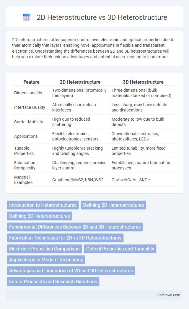
Table of Comparison
| Feature | 2D Heterostructure | 3D Heterostructure |
|---|---|---|
| Dimensionality | Two-dimensional (atomically thin layers) | Three-dimensional (bulk materials stacked or combined) |
| Interface Quality | Atomically sharp, clean interfaces | Less sharp, may have defects and dislocations |
| Carrier Mobility | High due to reduced scattering | Moderate to low due to bulk defects |
| Applications | Flexible electronics, optoelectronics, sensors | Conventional electronics, photovoltaics, LEDs |
| Tunable Properties | Highly tunable via stacking and twisting angles | Limited tunability, more fixed properties |
| Fabrication Complexity | Challenging, requires precise layer control | Established, mature fabrication processes |
| Material Examples | Graphene/MoS2, hBN/WS2 | GaAs/AlGaAs, Si/Ge |
Introduction to Heterostructures
Heterostructures are engineered materials formed by stacking layers of two or more semiconductors with differing electronic properties. 2D heterostructures consist of atomically thin layers with strong in-plane bonds and weak van der Waals interactions between layers, enabling precise control at the atomic scale. 3D heterostructures involve bulk materials with strain-induced interfaces, affecting carrier mobility and band alignment in complex ways that suit different electronic and optoelectronic applications.
Defining 2D Heterostructures
2D heterostructures are materials composed of atomically thin layers stacked with precise control over their electronic and optical properties, distinguishing them from traditional 3D heterostructures characterized by bulk material interfaces. The defining feature of 2D heterostructures lies in their van der Waals bonding between layers, enabling novel quantum phenomena and enhanced device performance at the nanoscale. You can leverage 2D heterostructures for applications requiring ultra-thin, flexible, and highly tunable electronic components.
Defining 3D Heterostructures
3D heterostructures refer to materials composed of different semiconductor layers stacked or integrated in three-dimensional configurations, enabling enhanced electronic and optoelectronic properties through spatially varied interfaces. Unlike 2D heterostructures that consist of atomically thin layers with van der Waals bonding, 3D heterostructures involve bulk materials with epitaxial growth techniques ensuring lattice matching and coherent interfaces. These structures are critical in high-performance devices like multi-junction solar cells and advanced transistors due to their superior charge carrier confinement and tunable band alignment across multiple layers.
Fundamental Differences Between 2D and 3D Heterostructures
2D heterostructures consist of atomically thin layers stacked vertically with strong in-plane covalent bonds and weak van der Waals forces between layers, enabling unique electronic and optical properties distinct from bulk materials. In contrast, 3D heterostructures are formed by epitaxial layers with covalent bonding in all three dimensions, resulting in thicker structures with different charge transport and strain characteristics. Your choice between 2D and 3D heterostructures depends on the desired application, such as flexible electronics or traditional semiconductor devices.
Fabrication Techniques for 2D vs 3D Heterostructures
Fabrication techniques for 2D heterostructures predominantly involve methods such as chemical vapor deposition (CVD), mechanical exfoliation, and molecular beam epitaxy (MBE) to achieve atomically thin layered materials with precise control over thickness and stacking order. In contrast, 3D heterostructure fabrication often relies on bulk growth methods like metallorganic chemical vapor deposition (MOCVD) and liquid phase epitaxy (LPE), which create layered materials with macroscopic thickness and complex interfaces. The atomic-scale precision in 2D heterostructure fabrication enables novel electronic and optical properties not easily attainable with conventional 3D heterostructure methods.
Electronic Properties Comparison
2D heterostructures exhibit unique electronic properties such as enhanced carrier mobility, tunable band gaps, and strong quantum confinement effects compared to 3D heterostructures. In 3D heterostructures, electronic behavior is influenced by bulk properties and strain effects, often resulting in less pronounced quantum confinement and reduced tunability. The atomically thin nature of 2D heterostructures enables superior interface control, leading to improved charge transfer efficiency and stronger excitonic effects than their 3D counterparts.
Optical Properties and Tunability
2D heterostructures exhibit superior optical properties due to their atomically thin layers, enabling strong light-matter interactions and enhanced exciton binding energies, which outperform those seen in bulk 3D heterostructures. The tunability in 2D materials is highly advanced, allowing precise control over bandgap and optical responses via stacking order, interlayer twist angles, and external stimuli like electric fields, providing customizable optical functionalities. Your applications can benefit from the exceptional tunability and efficient light absorption and emission characteristics inherent in 2D heterostructures compared to their 3D counterparts.
Applications in Modern Technology
2D heterostructures, composed of atomically thin layers like graphene and transition metal dichalcogenides, enable advanced electronic and optoelectronic devices such as flexible displays, sensors, and high-speed transistors due to their tunable band gaps and strong interlayer coupling. 3D heterostructures, built from bulk semiconductor materials like silicon-germanium or gallium arsenide, excel in traditional applications including power electronics, lasers, and photodetectors by providing robust structural integrity and well-established fabrication techniques. Your choice between 2D and 3D heterostructures impacts device performance, integration possibilities, and the scalability of next-generation technologies in fields like telecommunications and energy harvesting.
Advantages and Limitations of 2D and 3D Heterostructures
2D heterostructures offer superior control over interfacial properties and exhibit unique electronic and optical characteristics due to their atomic thickness, making them ideal for flexible and transparent electronics, but they face challenges in large-scale manufacturing and stability. In contrast, 3D heterostructures provide robust mechanical strength and are easier to integrate into existing semiconductor technologies but often suffer from less precise interfacial control and slower charge transport. Each structure type presents trade-offs between scalability, performance, and fabrication complexity crucial for applications in next-generation electronic and optoelectronic devices.
Future Prospects and Research Directions
2D heterostructures exhibit exceptional potential for next-generation electronics and optoelectronics due to their atomic-scale thickness and tunable interlayer interactions, enabling innovations like ultra-fast transistors and flexible devices. In contrast, 3D heterostructures offer robustness and integrated functionality for complex semiconductor applications but face scaling limitations. Your exploration of future research should prioritize hybrid systems that combine 2D and 3D advantages, targeting enhanced performance, novel quantum phenomena, and scalable manufacturing techniques.
2D Heterostructure vs 3D Heterostructure Infographic