Monolayer MoS2 exhibits a direct bandgap ideal for optoelectronic applications, while bilayer MoS2 has an indirect bandgap offering different electronic and mechanical properties. Explore the article to understand which MoS2 structure best suits your technology needs.
Table of Comparison
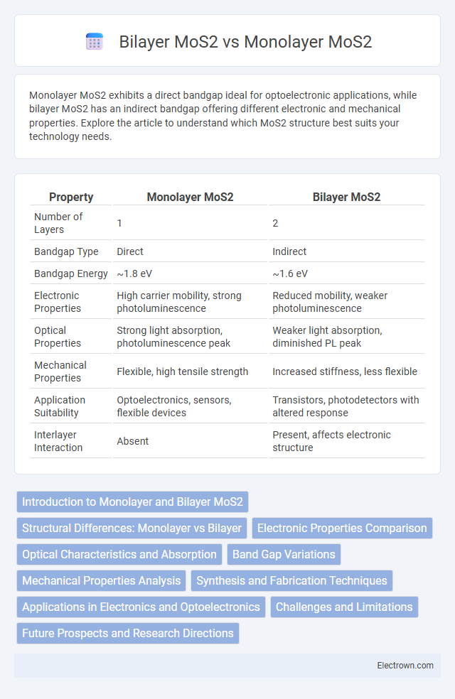
| Property | Monolayer MoS2 | Bilayer MoS2 |
|---|---|---|
| Number of Layers | 1 | 2 |
| Bandgap Type | Direct | Indirect |
| Bandgap Energy | ~1.8 eV | ~1.6 eV |
| Electronic Properties | High carrier mobility, strong photoluminescence | Reduced mobility, weaker photoluminescence |
| Optical Properties | Strong light absorption, photoluminescence peak | Weaker light absorption, diminished PL peak |
| Mechanical Properties | Flexible, high tensile strength | Increased stiffness, less flexible |
| Application Suitability | Optoelectronics, sensors, flexible devices | Transistors, photodetectors with altered response |
| Interlayer Interaction | Absent | Present, affects electronic structure |
Introduction to Monolayer and Bilayer MoS2
Monolayer MoS2 consists of a single layer of molybdenum atoms sandwiched between two layers of sulfur atoms, exhibiting a direct bandgap ideal for optoelectronic applications. Bilayer MoS2 features two stacked atomic layers with interlayer interactions causing an indirect bandgap, affecting its electronic and optical properties. Your choice between monolayer and bilayer MoS2 depends on desired conductivity, flexibility, and device performance parameters.
Structural Differences: Monolayer vs Bilayer
Monolayer MoS2 consists of a single layer of molybdenum atoms sandwiched between two layers of sulfur atoms, creating a hexagonal lattice with direct bandgap properties. Bilayer MoS2 features two such layers stacked via van der Waals forces, resulting in altered interlayer coupling and an indirect bandgap. Your choice between monolayer and bilayer MoS2 significantly affects electronic and optical behaviors due to these structural differences.
Electronic Properties Comparison
Monolayer MoS2 exhibits a direct bandgap of approximately 1.8 eV, making it highly efficient for optoelectronic applications and offering superior electron mobility compared to bilayer MoS2. Bilayer MoS2, with an indirect bandgap around 1.6 eV, shows reduced photoluminescence intensity and altered charge carrier dynamics due to interlayer coupling. Understanding these differences is crucial for optimizing your device performance in transistors, photodetectors, and flexible electronics.
Optical Characteristics and Absorption
Monolayer MoS2 exhibits a direct bandgap of around 1.8 eV, resulting in strong photoluminescence and higher optical absorption in the visible spectrum compared to bilayer MoS2. Bilayer MoS2 features an indirect bandgap near 1.6 eV, which reduces its photoluminescence efficiency and alters its absorption properties, making it less effective for optoelectronic applications. The enhanced excitonic effects and stronger light-matter interaction in monolayer MoS2 contribute to superior optical characteristics over the bilayer structure.
Band Gap Variations
Monolayer MoS2 exhibits a direct band gap of approximately 1.8 eV, making it highly efficient for optoelectronic applications such as photodetectors and LEDs. In contrast, Bilayer MoS2 features an indirect band gap around 1.2 eV, which diminishes its photoluminescence efficiency but improves its suitability for electronic devices where lower recombination rates are beneficial. Understanding these band gap variations allows you to tailor MoS2 layers for specific semiconductor applications based on energy conversion or charge transport needs.
Mechanical Properties Analysis
Monolayer MoS2 exhibits superior mechanical flexibility and higher tensile strength compared to bilayer MoS2, making it ideal for applications requiring lightweight and durable materials. Bilayer MoS2, while slightly less flexible, offers enhanced interlayer coupling that improves its fracture toughness and resistance to mechanical deformation. Understanding these distinctions can help you select the appropriate MoS2 configuration for specific strain-sensitive or flexible electronic devices.
Synthesis and Fabrication Techniques
Monolayer MoS2 is commonly synthesized via chemical vapor deposition (CVD) and mechanical exfoliation, offering high-quality, atomically thin films essential for electronic applications. Bilayer MoS2 often requires more precise control during growth, such as layer-by-layer CVD or liquid-phase exfoliation followed by stacking, to maintain uniform thickness and optimal interlayer coupling. Understanding these fabrication techniques helps you tailor material properties for specific device performance.
Applications in Electronics and Optoelectronics
Monolayer MoS2 exhibits a direct bandgap of approximately 1.8 eV, making it highly efficient for optoelectronic devices such as photodetectors and light-emitting diodes (LEDs). Bilayer MoS2 transitions to an indirect bandgap near 1.6 eV, which affects its electron mobility but enhances its suitability for field-effect transistors (FETs) requiring higher current on/off ratios. Both forms demonstrate promising applications in flexible electronics and nanoscale sensors, with monolayers optimizing light absorption and bilayers improving charge transport properties.
Challenges and Limitations
Monolayer MoS2 exhibits superior electronic and optical properties compared to bilayer MoS2, but its atomically thin nature leads to challenges such as environmental instability and difficulty in achieving uniform large-area synthesis. Bilayer MoS2, while offering improved mechanical robustness, faces limitations including reduced direct bandgap characteristics and interlayer coupling effects that degrade carrier mobility. Both forms encounter challenges in scalability and integration into practical devices due to defects, grain boundaries, and substrate interactions affecting overall performance.
Future Prospects and Research Directions
Monolayer MoS2 exhibits direct bandgap properties ideal for next-generation optoelectronics and flexible devices, whereas bilayer MoS2 with its tunable indirect bandgap offers promising applications in spintronics and valleytronics. Emerging research explores heterostructures combining monolayer and bilayer MoS2 to enhance electronic and photonic performance, aiming at scalable, energy-efficient technologies. Your advancements in controlling layer thickness and optimizing interlayer interactions will drive breakthroughs in wearable sensors, quantum computing, and nanoelectronics.
Monolayer MoS2 vs Bilayer MoS2 Infographic