Nanogap electrodes provide significantly enhanced sensitivity and selectivity in detecting molecular interactions compared to planar electrodes due to their ultra-small gap size, enabling precise electron tunneling measurements. Discover how choosing the right electrode type can impact your device performance by reading the rest of the article.
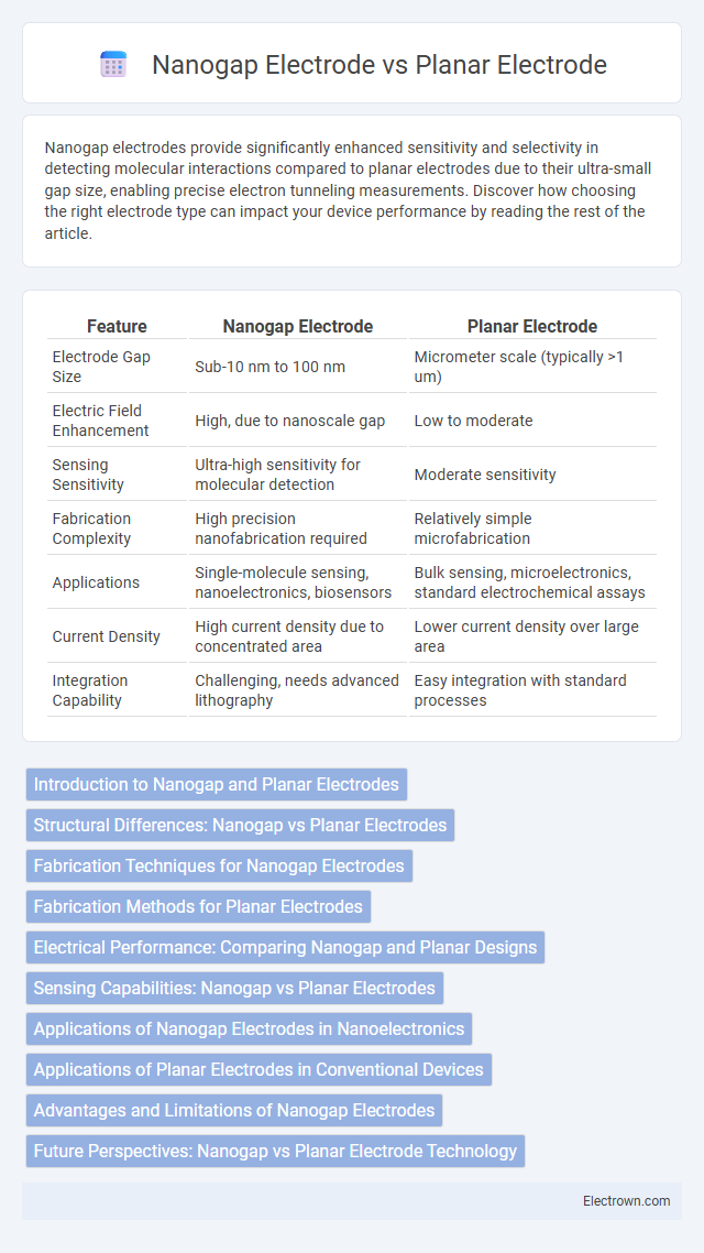
Table of Comparison
| Feature | Nanogap Electrode | Planar Electrode |
|---|---|---|
| Electrode Gap Size | Sub-10 nm to 100 nm | Micrometer scale (typically >1 um) |
| Electric Field Enhancement | High, due to nanoscale gap | Low to moderate |
| Sensing Sensitivity | Ultra-high sensitivity for molecular detection | Moderate sensitivity |
| Fabrication Complexity | High precision nanofabrication required | Relatively simple microfabrication |
| Applications | Single-molecule sensing, nanoelectronics, biosensors | Bulk sensing, microelectronics, standard electrochemical assays |
| Current Density | High current density due to concentrated area | Lower current density over large area |
| Integration Capability | Challenging, needs advanced lithography | Easy integration with standard processes |
Introduction to Nanogap and Planar Electrodes
Nanogap electrodes feature nanometer-scale separations enabling enhanced sensitivity and localized electric fields ideal for detecting biomolecules and nanoscale phenomena. Planar electrodes present a larger, flat surface area commonly used in traditional electrochemical sensors, offering ease of fabrication but lower spatial resolution. Your choice depends on the application's requirement for precision, sensing scale, and signal enhancement.
Structural Differences: Nanogap vs Planar Electrodes
Nanogap electrodes feature electrode pairs separated by nanometer-scale gaps, enabling extremely high electric field concentration and enhanced sensitivity for nanoelectronic and biosensing applications. Planar electrodes consist of flat surfaces with micrometer to millimeter gaps, providing simpler fabrication and larger active areas but lower field localization. The nanoscale gap dimension in nanogap electrodes results in unique electron tunneling and plasmonic effects absent in planar electrode configurations.
Fabrication Techniques for Nanogap Electrodes
Nanogap electrodes are fabricated using advanced techniques such as electron beam lithography, focused ion beam milling, and electromigration to achieve gap sizes below 10 nanometers, which surpasses the spatial resolution of planar electrode fabrication methods. In contrast, planar electrodes typically rely on conventional photolithography with larger feature sizes and simpler patterning processes. Your choice of fabrication technique directly influences the electrode's precision, electrical performance, and potential applications in nanoscale sensing and molecular electronics.
Fabrication Methods for Planar Electrodes
Planar electrodes are typically fabricated using photolithography combined with metal deposition techniques such as electron beam evaporation or sputtering, enabling precise patterning on substrates like silicon or glass. Thin films of conductive materials like gold, platinum, or copper are deposited and subsequently defined into electrode structures through lift-off or etching processes. These methods provide scalability and reproducibility critical for applications in biosensors, microelectronic devices, and electrochemical systems.
Electrical Performance: Comparing Nanogap and Planar Designs
Nanogap electrodes exhibit significantly enhanced electrical performance compared to planar electrodes due to their ultra-small electrode spacing, which enables stronger electric fields and more efficient charge transport. The reduced gap in nanogap electrodes minimizes resistance and capacitance, leading to improved signal sensitivity and faster response times in nanoscale devices. In contrast, planar electrodes with larger gaps typically suffer from lower electric field intensity and higher parasitic capacitance, limiting their performance in high-precision electronic applications.
Sensing Capabilities: Nanogap vs Planar Electrodes
Nanogap electrodes offer significantly enhanced sensing capabilities compared to planar electrodes due to their extremely small inter-electrode distances, allowing for higher sensitivity and improved detection of low-concentration analytes. The confined electric field in nanogap electrodes leads to enhanced signal-to-noise ratio and faster response times, making them ideal for applications requiring precise molecular detection. Your choice of electrode type directly impacts sensor performance, with nanogap designs providing superior accuracy and reliability in biochemical and environmental sensing applications.
Applications of Nanogap Electrodes in Nanoelectronics
Nanogap electrodes enable ultra-sensitive detection and manipulation of single molecules, making them essential in nanoelectronics for applications like molecular transistors and nanoscale sensors. Their precisely controlled, sub-10-nanometer gaps facilitate quantum tunneling and enhanced electrical characteristics, crucial for developing next-generation devices such as single-electron transistors and biosensors. Your ability to integrate nanogap electrodes into circuits enhances device performance by improving signal resolution and miniaturization beyond the limits of planar electrodes.
Applications of Planar Electrodes in Conventional Devices
Planar electrodes are widely used in conventional devices such as sensors, capacitors, and batteries due to their simple fabrication and reliable performance. These electrodes offer uniform electric fields and efficient charge transfer, making them ideal for applications in electrochemical sensing, energy storage, and microelectronics. Your device's stability and reproducibility benefit significantly from the well-established planar electrode designs in these traditional systems.
Advantages and Limitations of Nanogap Electrodes
Nanogap electrodes offer exceptional sensitivity and precision in detecting molecular-scale changes due to their extremely small gap sizes, making them ideal for applications like single-molecule electronics and biosensing. Their primary advantage lies in enhanced signal resolution and reduced sample volume requirements, though fabrication complexity and stability challenges limit widespread adoption compared to planar electrodes. Your choice depends on whether the improved performance of nanogap electrodes outweighs the manufacturing difficulties associated with their nanoscale features.
Future Perspectives: Nanogap vs Planar Electrode Technology
Nanogap electrodes offer unprecedented opportunities for ultra-sensitive molecular detection and quantum device integration due to their sub-10 nm gap precision and enhanced electric field concentration. In contrast, planar electrodes, with their mature fabrication methods and scalability, remain favorable for large-scale electronic applications but face limitations in achieving nanoscale resolution. Future advancements are likely to merge nanogap precision with planar electrode scalability, driving innovations in nanoelectronics, biosensing, and quantum computing platforms.
Nanogap electrode vs Planar electrode Infographic