Schottky contacts create a rectifying junction with a metal-semiconductor interface, allowing current to flow primarily in one direction, while ohmic contacts provide a low-resistance, bidirectional connection essential for efficient charge injection. Explore the article to understand how these contacts impact your device's performance and application.
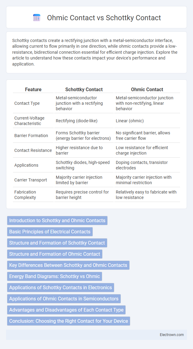
Table of Comparison
| Feature | Schottky Contact | Ohmic Contact |
|---|---|---|
| Contact Type | Metal-semiconductor junction with a rectifying behavior | Metal-semiconductor junction with non-rectifying, linear behavior |
| Current-Voltage Characteristic | Rectifying (diode-like) | Linear (ohmic) |
| Barrier Formation | Forms Schottky barrier (energy barrier for electrons) | No significant barrier, allows free carrier flow |
| Contact Resistance | Higher resistance due to barrier | Low resistance for efficient charge injection |
| Applications | Schottky diodes, high-speed switching | Doping contacts, transistor electrodes |
| Carrier Transport | Majority carrier injection limited by barrier | Majority carrier injection with minimal restriction |
| Fabrication Complexity | Requires precise control for barrier height | Relatively easy to fabricate with low resistance |
Introduction to Schottky and Ohmic Contacts
Schottky contacts are metal-semiconductor interfaces that form rectifying junctions, allowing current to flow primarily in one direction and are essential in high-speed switching devices. Ohmic contacts, on the other hand, provide low-resistance, non-rectifying connections essential for efficient current injection and extraction in semiconductor devices. Understanding the differences in barrier formation and electrical behavior between Schottky and Ohmic contacts is crucial for optimizing your device performance and reliability.
Basic Principles of Electrical Contacts
Schottky contacts form a metal-semiconductor junction with a built-in potential barrier that controls electron flow, enabling rectifying behavior essential for diodes and high-speed switching devices. Ohmic contacts provide a low-resistance, non-rectifying interface, allowing efficient current injection into the semiconductor for reliable device operation. Understanding these basic principles ensures your electronic components achieve optimal performance through appropriate contact selection.
Structure and Formation of Schottky Contact
Schottky contacts form at the metal-semiconductor interface, creating a rectifying barrier due to the energy band alignment between the metal work function and semiconductor electron affinity. The structure involves a thin metal layer deposited on an n-type or p-type semiconductor, resulting in a depletion region that controls charge carrier flow. Your device's performance depends on precisely controlling this contact formation to tailor the barrier height and electric field distribution, distinguishing it from the low-resistance, non-rectifying ohmic contact.
Structure and Formation of Ohmic Contact
Ohmic contacts are formed by creating a low-resistance junction between a metal and a semiconductor, often achieved through heavy doping of the semiconductor region beneath the contact to facilitate tunneling. The structure typically consists of a metal layer deposited on a heavily doped semiconductor layer, allowing for a linear current-voltage (I-V) relationship without significant energy barriers. Unlike Schottky contacts, which form rectifying junctions due to the metal-semiconductor work function difference, ohmic contacts provide efficient charge carrier injection essential for device performance.
Key Differences Between Schottky and Ohmic Contacts
Schottky contacts form a metal-semiconductor junction with a rectifying behavior, characterized by a built-in potential barrier that allows current to flow primarily in one direction, ideal for high-speed switching applications. Ohmic contacts, in contrast, provide a low-resistance, non-rectifying interface that ensures efficient current injection and extraction without significant voltage drop, crucial for device performance stability. The key differences lie in their electrical behavior, contact resistance, and applications: Schottky contacts prominently feature a Schottky barrier height affecting current flow, whereas Ohmic contacts exhibit nearly linear I-V characteristics due to minimal contact resistance.
Energy Band Diagrams: Schottky vs Ohmic
The energy band diagram of a Schottky contact features a metal-semiconductor junction with a distinct potential barrier, the Schottky barrier height, which restricts electron flow and creates rectifying behavior. In contrast, an Ohmic contact displays minimal or no barrier in its band diagram, allowing charge carriers to move freely across the metal-semiconductor interface, resulting in linear current-voltage characteristics. The key difference lies in the alignment of the metal's work function and the semiconductor's electron affinity, dictating the band bending and thus the barrier formation in Schottky versus the seamless carrier injection in Ohmic contacts.
Applications of Schottky Contacts in Electronics
Schottky contacts are widely used in high-speed switching applications, such as in Schottky diodes for power rectification due to their low forward voltage drop and fast recovery time. They are essential in radio frequency (RF) circuits and microwave devices, improving efficiency and signal integrity. Schottky contacts also serve as critical components in metal-semiconductor field-effect transistors (MESFETs) and photodetectors, benefiting from their rectifying characteristics and low capacitance.
Applications of Ohmic Contacts in Semiconductors
Ohmic contacts are essential in semiconductor devices for establishing low-resistance electrical connections between metal electrodes and semiconductor materials, ensuring efficient current injection and extraction. They are widely used in integrated circuits, solar cells, and transistors to enable reliable signal transmission and power delivery. Their ability to provide linear I-V characteristics without rectification is crucial for device performance and durability.
Advantages and Disadvantages of Each Contact Type
Schottky contacts offer low forward voltage drop and fast switching speed, making them ideal for high-frequency applications, but they exhibit significant reverse leakage current and poor linearity. Ohmic contacts provide excellent current conduction with minimal resistance and negligible rectification, ensuring efficient charge injection, yet they often require complex fabrication processes and may have higher contact resistance at nanoscale dimensions. Selecting between Schottky and Ohmic contacts depends on the balance between desired electrical performance and fabrication complexity in semiconductor devices.
Conclusion: Choosing the Right Contact for Your Device
Selecting the appropriate contact for your device depends on the desired electrical behavior: Schottky contacts provide rectifying characteristics with low forward voltage and fast switching ideal for high-speed and low-power applications, while Ohmic contacts ensure linear current-voltage response critical for efficient charge injection and extraction in devices like transistors and photodetectors. Material compatibility, barrier height, and fabrication complexity influence the choice, where Schottky contacts require metals with suitable work functions to control barrier formation, and Ohmic contacts often use heavily doped semiconductors for minimal contact resistance. Optimizing contact type enhances device performance, longevity, and energy efficiency tailored to specific application requirements in semiconductor technology.
Schottky Contact vs Ohmic Contact Infographic