Nanophotonics explores light-matter interactions at the nanoscale, enabling breakthroughs in imaging, sensing, and communication technologies, while optoelectronics focuses on devices that convert electrical signals into optical signals and vice versa, such as LEDs and photodetectors. Discover how understanding these distinct yet interconnected fields can enhance your knowledge of next-generation photonic devices in the rest of this article.
Table of Comparison
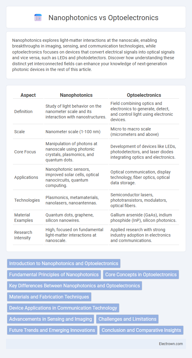
| Aspect | Nanophotonics | Optoelectronics |
|---|---|---|
| Definition | Study of light behavior on the nanometer scale and its interaction with nanostructures. | Field combining optics and electronics to generate, detect, and control light using electronic devices. |
| Scale | Nanometer scale (1-100 nm) | Micro to macro scale (micrometers and above) |
| Core Focus | Manipulation of photons at nanoscale using photonic crystals, plasmonics, and quantum dots. | Development of devices like LEDs, photodetectors, and laser diodes integrating optics and electronics. |
| Applications | Nanophotonic sensors, improved solar cells, optical nanocircuits, quantum computing. | Optical communication, display technology, fiber optics, optical data storage. |
| Technologies | Plasmonics, metamaterials, nanolasers, nanoantennas. | Semiconductor lasers, phototransistors, modulators, optical fibers. |
| Material Examples | Quantum dots, graphene, silicon nanowires. | Gallium arsenide (GaAs), indium phosphide (InP), silicon photonics. |
| Research Intensity | High, focused on fundamental light-matter interactions at nanoscale. | Applied research with strong industry adoption in electronics and communications. |
Introduction to Nanophotonics and Optoelectronics
Nanophotonics explores the behavior of light on the nanometer scale, enabling innovations in manipulating photons within nanostructures. Optoelectronics involves devices that convert electrical signals into photon signals and vice versa, integrating optical and electronic functionalities for applications such as sensors, communication, and displays. Your understanding of these fields reveals how nanophotonics enhances device miniaturization while optoelectronics drives the development of efficient light-based technologies.
Fundamental Principles of Nanophotonics
Nanophotonics explores light behavior and interaction with matter at the nanometer scale, relying on principles such as quantum optics, plasmonics, and photonic crystals to manipulate photons beyond the diffraction limit. This field leverages nanoscale structures to control electromagnetic fields with high precision, enabling devices with enhanced light-matter interaction efficiency. Understanding these fundamental principles helps you innovate in applications like optical sensors, communication, and energy harvesting at unprecedented miniaturization levels.
Core Concepts in Optoelectronics
Optoelectronics centers on the interaction between light and electronic devices, primarily involving components like photodiodes, LEDs, and laser diodes used for signal conversion and modulation. Core concepts include light emission, detection, and optical signal processing, relying on semiconductor materials to control electron-hole recombination and photon generation. These principles enable applications in fiber optic communication, display technology, and optical sensing systems.
Key Differences Between Nanophotonics and Optoelectronics
Nanophotonics studies light behavior on the nanometer scale, manipulating photons in structures smaller than the wavelength of light, enabling breakthroughs in imaging, sensing, and quantum computing. Optoelectronics integrates electronic and optical processes, focusing on devices like LEDs, photodiodes, and lasers that convert electrical signals into optical signals and vice versa. Understanding these key differences helps you choose the right technology for applications requiring nanoscale light control or electronic-optical signal conversion.
Materials and Fabrication Techniques
Nanophotonics relies on advanced materials such as plasmonic metals, dielectric nanoparticles, and 2D materials like graphene, fabricated using techniques including electron beam lithography, focused ion beam milling, and atomic layer deposition to achieve nanoscale control of light-matter interactions. Optoelectronics utilizes semiconductor materials like gallium arsenide, indium phosphide, and silicon, with fabrication processes based on photolithography, epitaxial growth, and chemical vapor deposition tailored for integrated photonic devices and light emission applications. The choice of materials and fabrication methods directly influences device performance, pushing nanophotonics toward ultra-compact, high-speed optical components and optoelectronics toward efficient, scalable photonic-electronic integration.
Device Applications in Communication Technology
Nanophotonics enables ultra-compact, high-speed optical communication devices by manipulating light at the nanoscale, significantly improving data transmission rates and energy efficiency. Optoelectronics integrates electronic and photonic components to convert electrical signals into optical ones and vice versa, supporting fiber-optic networks and optical modulators essential for broadband communication. Your choice between these technologies depends on the desired device miniaturization, speed, and integration complexity in modern communication systems.
Advancements in Sensing and Imaging
Nanophotonics enhances sensing and imaging by manipulating light at the nanoscale, enabling unprecedented spatial resolution and sensitivity in detecting biological and chemical substances. Optoelectronics integrates electronic and photonic components to improve imaging systems' speed and accuracy, crucial for medical diagnostics and environmental monitoring. Your ability to leverage these advancements can lead to highly precise, real-time analysis in various scientific and industrial applications.
Challenges and Limitations
Nanophotonics faces challenges in manipulating light at the nanoscale due to inherent material losses and fabrication precision limits, impacting device efficiency and scalability. Optoelectronics struggles with integrating diverse materials and managing thermal effects, which constrain performance and lifetime in practical applications. Your choice between nanophotonics and optoelectronics must consider these limitations to optimize functionality and reliability.
Future Trends and Emerging Innovations
Nanophotonics is advancing with breakthroughs like quantum dot lasers and metasurfaces that manipulate light at the nanoscale, driving ultra-fast optical computing and high-resolution imaging. Optoelectronics is evolving through innovations in flexible photodetectors, integrated photonic circuits, and energy-efficient light-emitting diodes, enhancing communication technologies and wearable devices. Your ability to harness these emerging technologies will shape future developments in high-speed data transmission and smart sensing applications.
Conclusion and Comparative Insights
Nanophotonics explores light behavior at the nanometer scale, enabling innovations in imaging, sensing, and quantum computing, while optoelectronics focuses on devices that convert electrical signals into light and vice versa, essential for communication and display technologies. Your choice between these fields depends on whether you aim to manipulate light at ultra-small scales for fundamental research or develop practical light-based electronic devices for commercial applications. Both areas offer transformative potential, with nanophotonics driving breakthroughs in miniaturization and optoelectronics advancing efficient, high-speed data transmission.
Nanophotonics vs Optoelectronics Infographic