Monolayer nanosheets consist of a single atomic or molecular layer, offering exceptional electronic, optical, and mechanical properties due to their minimal thickness and high surface area, whereas multilayer nanosheets contain stacked layers, which influence their conductivity and chemical stability. Explore the rest of the article to understand how these differences impact your applications in nanotechnology and material science.
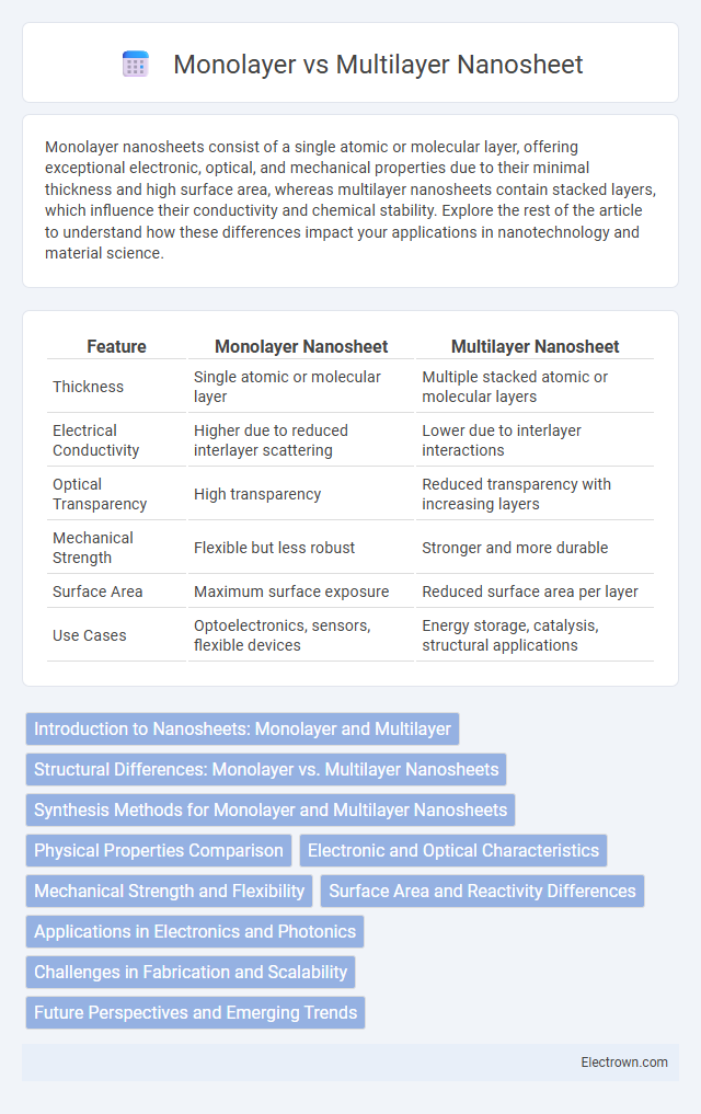
Table of Comparison
| Feature | Monolayer Nanosheet | Multilayer Nanosheet |
|---|---|---|
| Thickness | Single atomic or molecular layer | Multiple stacked atomic or molecular layers |
| Electrical Conductivity | Higher due to reduced interlayer scattering | Lower due to interlayer interactions |
| Optical Transparency | High transparency | Reduced transparency with increasing layers |
| Mechanical Strength | Flexible but less robust | Stronger and more durable |
| Surface Area | Maximum surface exposure | Reduced surface area per layer |
| Use Cases | Optoelectronics, sensors, flexible devices | Energy storage, catalysis, structural applications |
Introduction to Nanosheets: Monolayer and Multilayer
Nanosheets are atomically thin materials with unique physical and chemical properties that vary significantly between monolayer and multilayer forms. Monolayer nanosheets consist of a single atomic layer, offering exceptional electrical conductivity, mechanical flexibility, and quantum effects that enhance performance in electronics and catalysis. Multilayer nanosheets, composed of multiple stacked layers, exhibit modified optical properties, increased structural stability, and tunable interlayer interactions useful in energy storage and sensing applications.
Structural Differences: Monolayer vs. Multilayer Nanosheets
Monolayer nanosheets consist of a single atomic or molecular layer, resulting in unique electronic and optical properties due to quantum confinement and increased surface area. Multilayer nanosheets are composed of several stacked layers held together by van der Waals forces, which affect their mechanical strength and electrical conductivity by introducing interlayer coupling. Understanding these structural differences helps optimize your nanosheet selection for applications in sensors, electronics, and catalysis.
Synthesis Methods for Monolayer and Multilayer Nanosheets
Chemical vapor deposition (CVD) and mechanical exfoliation are prominent synthesis methods for monolayer nanosheets, enabling precise control over layer thickness and high crystallinity. In contrast, multilayer nanosheets are often produced using liquid-phase exfoliation and layer-by-layer assembly, facilitating scalable production with tunable layer numbers. Advanced techniques like molecular beam epitaxy (MBE) enhance the uniformity and quality of both monolayer and multilayer nanosheets, critical for electronic and optoelectronic applications.
Physical Properties Comparison
Monolayer nanosheets exhibit exceptional mechanical flexibility, higher transparency, and superior electron mobility compared to multilayer nanosheets, which tend to have increased thickness and enhanced mechanical strength but reduced optical clarity and conductivity. The reduced interlayer interactions in monolayers result in unique quantum properties, whereas multilayers provide improved thermal stability and stiffness due to van der Waals forces between layers. Understanding these distinctions helps optimize your choice of nanosheet for applications requiring either high transparency and mobility or robust structural integrity.
Electronic and Optical Characteristics
Monolayer nanosheets exhibit superior electronic properties such as higher carrier mobility and direct bandgaps, enabling enhanced optical absorption and efficient light emission ideal for optoelectronic devices. Multilayer nanosheets often show indirect bandgaps with reduced carrier mobility, resulting in diminished photoluminescence intensity and altered excitonic behavior. Understanding these distinctions helps you tailor nanosheet materials for specific electronic and photonic applications.
Mechanical Strength and Flexibility
Monolayer nanosheets exhibit exceptional flexibility due to their single atomic layer structure, allowing significant bending without breaking, while multilayer nanosheets generally provide enhanced mechanical strength resulting from interlayer interactions and stacking. Your choice between monolayer and multilayer nanosheets depends on whether flexibility or mechanical robustness is more critical for your application. Multilayer nanosheets also tend to have increased resistance to mechanical deformation but at the cost of reduced flexibility compared to monolayers.
Surface Area and Reactivity Differences
Monolayer nanosheets exhibit significantly higher surface area compared to multilayer nanosheets, enhancing their reactivity and catalytic efficiency due to increased exposure of active sites. Multilayer nanosheets have reduced surface accessibility, which limits interaction with reactants and results in lower chemical reactivity. Your choice between monolayer and multilayer nanosheets depends on the desired balance between surface area-driven reactivity and structural stability.
Applications in Electronics and Photonics
Monolayer nanosheets exhibit exceptional electron mobility and direct bandgap properties, making them ideal for high-performance transistors, flexible displays, and photodetectors in electronics. Multilayer nanosheets offer tunable bandgaps and enhanced interlayer coupling, which are critical for optoelectronic devices such as solar cells, light-emitting diodes (LEDs), and modulators in photonics. Both materials enable advances in nanoelectronics and integrated photonic circuits due to their unique thickness-dependent optical and electrical characteristics.
Challenges in Fabrication and Scalability
Fabrication of monolayer nanosheets faces challenges such as controlling uniform thickness at the atomic scale and preventing defects during synthesis, which limits scalability and consistent material quality. Multilayer nanosheets, while easier to produce in bulk via methods like chemical vapor deposition (CVD) or liquid-phase exfoliation, encounter issues with interlayer stacking faults and maintaining layer uniformity, impacting electronic and optical properties. Scaling both monolayer and multilayer nanosheets requires advancements in precise control over growth parameters and cost-effective, large-area production techniques to enable industrial applications.
Future Perspectives and Emerging Trends
Future perspectives in monolayer versus multilayer nanosheets highlight their evolving roles in next-generation electronics and energy storage, with monolayers offering superior electronic conductivity and sensitivity due to their atomic thickness. Emerging trends emphasize the integration of multilayer nanosheets for enhanced mechanical stability and tunable optical properties, driving innovation in flexible devices and photonics. Advances in scalable synthesis methods and heterostructure engineering are pivotal for optimizing performance tailored to specific applications across nanotechnology and materials science.
Monolayer VS Multilayer Nanosheet Infographic