Metallic nanotubes exhibit high electrical conductivity ideal for nanoelectronics, while semiconducting nanotubes offer tunable electronic properties crucial for transistors and sensors. Explore the rest of the article to understand how your choice between these nanotubes impacts device performance and application.
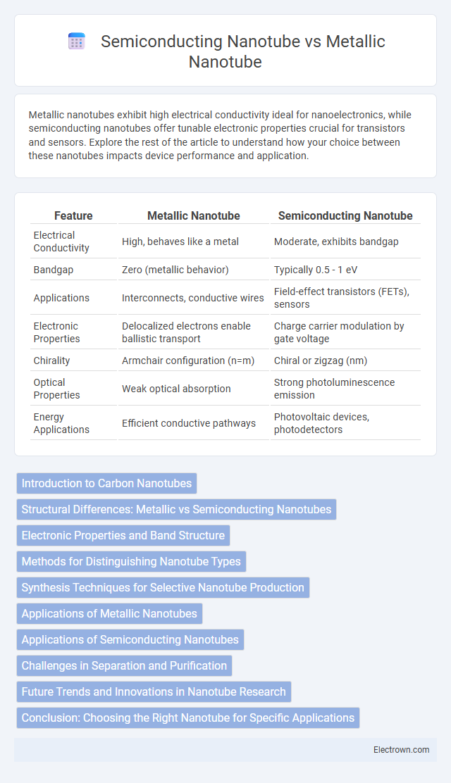
Table of Comparison
| Feature | Metallic Nanotube | Semiconducting Nanotube |
|---|---|---|
| Electrical Conductivity | High, behaves like a metal | Moderate, exhibits bandgap |
| Bandgap | Zero (metallic behavior) | Typically 0.5 - 1 eV |
| Applications | Interconnects, conductive wires | Field-effect transistors (FETs), sensors |
| Electronic Properties | Delocalized electrons enable ballistic transport | Charge carrier modulation by gate voltage |
| Chirality | Armchair configuration (n=m) | Chiral or zigzag (nm) |
| Optical Properties | Weak optical absorption | Strong photoluminescence emission |
| Energy Applications | Efficient conductive pathways | Photovoltaic devices, photodetectors |
Introduction to Carbon Nanotubes
Carbon nanotubes (CNTs) consist of cylindrical carbon molecules classified into metallic and semiconducting types based on their electronic properties. Metallic nanotubes exhibit excellent electrical conductivity, making them ideal for nanoelectronic interconnects and conductive materials. Semiconducting nanotubes possess a bandgap, which enables their use in transistors, sensors, and nanoscale electronic devices, tailoring Your applications to specific technological needs.
Structural Differences: Metallic vs Semiconducting Nanotubes
Metallic nanotubes feature armchair or certain chiral structures that allow free electron movement, resulting in high electrical conductivity. Semiconducting nanotubes possess zigzag or other chiral geometries that create band gaps, restricting electron flow and enabling transistor-like behavior. Your choice depends on whether you need highly conductive pathways or controlled electron transport for electronic applications.
Electronic Properties and Band Structure
Metallic nanotubes exhibit zero bandgap with continuous electronic states, allowing free electron flow and high electrical conductivity essential for nanoscale interconnects. Semiconducting nanotubes possess a finite bandgap, typically ranging from 0.5 to 2 eV, enabling bandgap-dependent electron transport properties critical for transistor channels and optoelectronic applications. The differing band structures arise from variations in chiral vectors and tube diameters, dictating whether the carbon nanotube behaves as a metal or semiconductor in nanoelectronic devices.
Methods for Distinguishing Nanotube Types
Distinguishing metallic nanotubes from semiconducting nanotubes involves techniques like Raman spectroscopy, which identifies vibrational modes characteristic to electronic properties, and photoluminescence spectroscopy, effective for detecting semiconducting nanotubes due to their light emission under excitation. Another method uses electrical measurement through field-effect transistors, where semiconducting nanotubes show gate voltage-dependent conductivity, unlike metallic nanotubes. Your choice of method depends on the precision required and the specific application of the nanotubes in electronics or sensing devices.
Synthesis Techniques for Selective Nanotube Production
Synthesis techniques for selective production of metallic and semiconducting nanotubes include chemical vapor deposition (CVD) with catalyst engineering and controlled growth environment. Methods like chirality-specific catalyst design and temperature modulation enable precise control over nanotube electronic properties during synthesis. Your choice of synthesis parameters directly influences the yield of desired metallic or semiconducting nanotube types for tailored applications.
Applications of Metallic Nanotubes
Metallic nanotubes exhibit excellent electrical conductivity, making them ideal for applications in nanoelectronics, such as interconnects in integrated circuits and conductive wiring in nanoscale devices. Their high current-carrying capacity and thermal conductivity enable use in field-effect transistors and nanosensors, enhancing device performance and sensitivity. Metallic nanotubes also serve as key components in energy storage systems, including supercapacitors and batteries, due to their efficient electron transport properties.
Applications of Semiconducting Nanotubes
Semiconducting nanotubes are pivotal in advanced electronics due to their exceptional electrical properties, enabling their use in field-effect transistors (FETs), sensors, and photodetectors. Their tunable bandgap allows precise control over electrical conductivity, making them ideal for flexible, high-performance nanoelectronic devices and optoelectronic applications. Your development projects can benefit from these nanotubes in creating efficient, miniaturized components with enhanced sensitivity and energy efficiency.
Challenges in Separation and Purification
Metallic nanotubes and semiconducting nanotubes pose significant challenges in separation and purification due to their similar physical dimensions and chemical properties. Techniques such as density gradient ultracentrifugation and selective chemical functionalization aim to isolate these nanotubes but often suffer from scalability issues and incomplete selectivity. Your ability to utilize high-purity semiconducting nanotubes for electronics hinges on overcoming these separation bottlenecks to achieve consistent material quality.
Future Trends and Innovations in Nanotube Research
Future trends in metallic and semiconducting nanotube research emphasize enhancing electron mobility and tunable bandgap properties for next-generation nanoelectronics and optoelectronics. Innovations include integrating carbon nanotubes with two-dimensional materials like graphene and transition metal dichalcogenides to create hybrid devices with superior electrical and thermal performance. Research also targets scalable synthesis methods and precise control over chirality to optimize the application-specific functionalities of nanotubes in flexible electronics, quantum computing, and energy storage systems.
Conclusion: Choosing the Right Nanotube for Specific Applications
Metallic nanotubes offer excellent electrical conductivity, making them ideal for applications in nanoelectronics and conductive wiring, while semiconducting nanotubes provide tunable band gaps essential for transistors and sensors. Your choice depends on whether electrical conductivity or semiconducting properties are critical for performance in devices like field-effect transistors or nanoscale interconnects. Considering the unique electrical characteristics of each nanotube type ensures optimal functionality tailored to specific technological needs.
Metallic Nanotube vs Semiconducting Nanotube Infographic