Schottky Barrier Transistors leverage metal-semiconductor junctions to achieve fast switching speeds and reduced contact resistance, while Junctionless Transistors eliminate p-n junctions entirely, offering simplified fabrication and better control over short-channel effects. To explore how these differences impact your device performance and application suitability, continue reading the detailed comparison in the article.
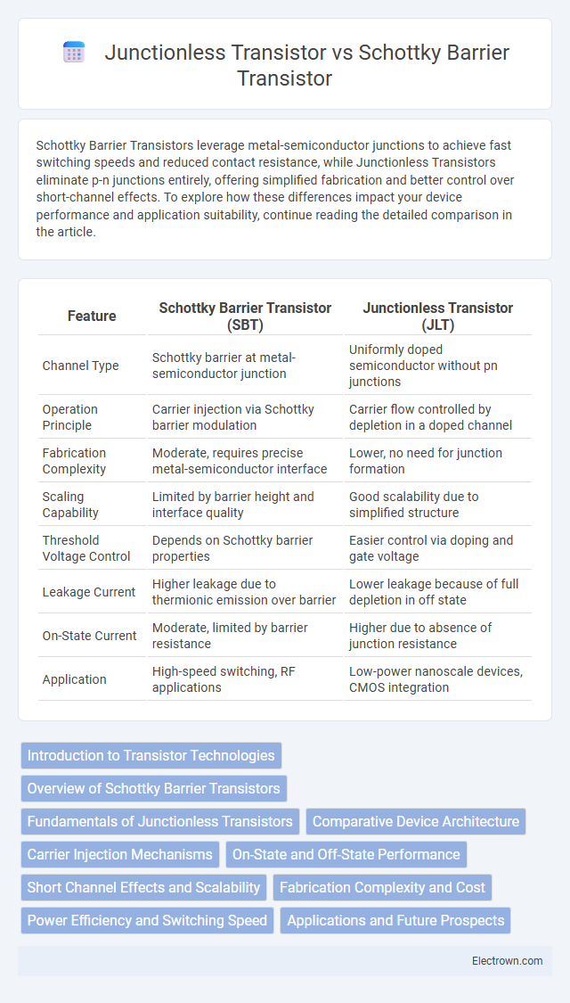
Table of Comparison
| Feature | Schottky Barrier Transistor (SBT) | Junctionless Transistor (JLT) |
|---|---|---|
| Channel Type | Schottky barrier at metal-semiconductor junction | Uniformly doped semiconductor without pn junctions |
| Operation Principle | Carrier injection via Schottky barrier modulation | Carrier flow controlled by depletion in a doped channel |
| Fabrication Complexity | Moderate, requires precise metal-semiconductor interface | Lower, no need for junction formation |
| Scaling Capability | Limited by barrier height and interface quality | Good scalability due to simplified structure |
| Threshold Voltage Control | Depends on Schottky barrier properties | Easier control via doping and gate voltage |
| Leakage Current | Higher leakage due to thermionic emission over barrier | Lower leakage because of full depletion in off state |
| On-State Current | Moderate, limited by barrier resistance | Higher due to absence of junction resistance |
| Application | High-speed switching, RF applications | Low-power nanoscale devices, CMOS integration |
Introduction to Transistor Technologies
Schottky Barrier Transistors utilize metal-semiconductor junctions to control current flow through Schottky barriers, offering faster switching speeds and lower power consumption compared to traditional devices. Junctionless Transistors eliminate the need for p-n junctions by using a uniformly doped channel, enhancing scalability and simplifying fabrication processes in advanced semiconductor technologies. Your choice between these transistors depends on application demands for speed, power efficiency, and manufacturing complexity.
Overview of Schottky Barrier Transistors
Schottky Barrier Transistors utilize a metal-semiconductor junction to form the channel, enabling faster switching speeds and lower power consumption compared to traditional junction-based devices. The Schottky barrier height at the metal-semiconductor interface directly influences carrier injection efficiency, impacting device performance and scalability in nanoelectronics. Your choice of Schottky Barrier Transistors can enhance device reliability in high-frequency applications due to their reduced parasitic capacitance and improved thermal stability.
Fundamentals of Junctionless Transistors
Junctionless transistors operate on the principle of a uniformly doped semiconductor channel without source/drain junctions, eliminating the need for abrupt doping profiles found in Schottky barrier transistors. They rely on electrostatic control through a gate electrode to modulate carrier concentration, reducing short-channel effects and enhancing device scalability. The absence of junctions simplifies fabrication and improves reliability, offering a promising alternative for future nanoelectronic applications.
Comparative Device Architecture
Schottky Barrier Transistors feature metal-semiconductor junctions that form Schottky barriers, enabling controlled carrier injection with reduced contact resistance, while Junctionless Transistors rely on a uniformly doped channel without traditional p-n junctions, minimizing short-channel effects and simplifying fabrication. The metal-semiconductor interface in Schottky devices leads to distinct energy barriers influencing carrier transport, whereas the Junctionless design utilizes a fully depleted channel to modulate current flow through electrostatic control. These architectural differences impact scalability, leakage current, and switching speed, positioning Junctionless Transistors as promising candidates for ultra-scaled applications with enhanced electrostatic integrity.
Carrier Injection Mechanisms
Schottky Barrier Transistors utilize metal-semiconductor junctions where carrier injection depends on tunneling through or thermionic emission over the Schottky barrier, enabling efficient charge transfer at the contact interface. Junctionless Transistors rely on uniform doping profiles throughout the channel, with carrier injection governed by bulk conduction without the need for traditional p-n junctions, reducing variability and short-channel effects. Your choice between these devices impacts the carrier injection efficiency and device performance in nanoscale electronics.
On-State and Off-State Performance
Schottky Barrier Transistors exhibit low on-state resistance due to their metal-semiconductor junctions, enabling faster switching speeds and efficient current conduction, while their off-state leakage currents can be higher compared to traditional transistors. Junctionless Transistors, lacking a p-n junction, provide excellent off-state performance with reduced leakage currents and improved electrostatic control, yet they may have relatively higher on-state resistance, impacting drive current. The trade-off between these two devices hinges on balancing on-state conductivity and off-state leakage, making them suitable for different applications in low-power and high-speed electronics.
Short Channel Effects and Scalability
Schottky Barrier Transistors face challenges with short channel effects due to the metal-semiconductor interface causing increased leakage currents and reduced gate control, limiting their scalability for advanced nodes. Junctionless Transistors mitigate short channel effects by using uniform doping and a gate-all-around structure that enhances electrostatic control, enabling better scalability in nanoscale technologies. Your choice between these devices should consider the trade-offs in leakage behavior and ease of fabrication when targeting highly scaled semiconductor devices.
Fabrication Complexity and Cost
Schottky Barrier Transistors require precise metal-semiconductor interface engineering, increasing fabrication complexity and cost due to specialized deposition and patterning processes. Junctionless Transistors simplify fabrication by eliminating doping gradients and PN junctions, reducing process steps and associated costs. The reduced reliance on precise doping control in junctionless designs makes them more cost-effective for large-scale production compared to Schottky Barrier Transistors.
Power Efficiency and Switching Speed
Schottky Barrier Transistors (SBTs) exhibit superior switching speed due to their low barrier height and reduced carrier transit time, enabling faster gate control and lower power consumption during high-frequency operations. Junctionless Transistors (JLTs) offer enhanced power efficiency by eliminating junction doping gradients, which reduces short-channel effects and leakage currents, prolonging battery life in portable devices. Your choice between the two should consider the need for rapid switching performance with SBTs or energy-efficient operation with JLTs, depending on application-specific power and speed requirements.
Applications and Future Prospects
Schottky Barrier Transistors excel in high-speed switching and low-power radio frequency applications due to their ultra-fast carrier injection and minimal contact resistance. Junctionless Transistors are promising for next-generation logic circuits and flexible electronics, offering simplified fabrication and enhanced scalability without the need for junction formation. Future prospects include integrating Schottky devices in advanced RF systems and leveraging junctionless designs for energy-efficient, highly scalable semiconductor technologies.
Schottky Barrier Transistor vs Junctionless Transistor Infographic