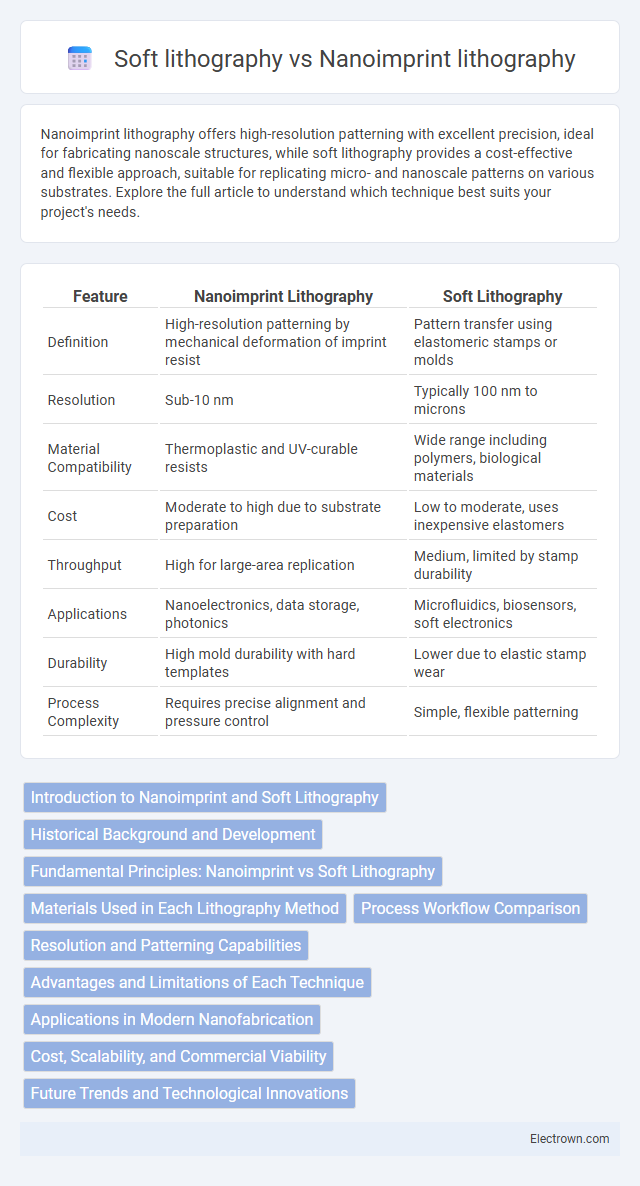
Nanoimprint lithography offers high-resolution patterning with excellent precision, ideal for fabricating nanoscale structures, while soft lithography provides a cost-effective and flexible approach, suitable for replicating micro- and nanoscale patterns on various substrates. Explore the full article to understand which technique best suits your project's needs.
Table of Comparison
| Feature | Nanoimprint Lithography | Soft Lithography |
|---|---|---|
| Definition | High-resolution patterning by mechanical deformation of imprint resist | Pattern transfer using elastomeric stamps or molds |
| Resolution | Sub-10 nm | Typically 100 nm to microns |
| Material Compatibility | Thermoplastic and UV-curable resists | Wide range including polymers, biological materials |
| Cost | Moderate to high due to substrate preparation | Low to moderate, uses inexpensive elastomers |
| Throughput | High for large-area replication | Medium, limited by stamp durability |
| Applications | Nanoelectronics, data storage, photonics | Microfluidics, biosensors, soft electronics |
| Durability | High mold durability with hard templates | Lower due to elastic stamp wear |
| Process Complexity | Requires precise alignment and pressure control | Simple, flexible patterning |
Introduction to Nanoimprint and Soft Lithography
Nanoimprint lithography (NIL) is a high-resolution patterning technique that uses mechanical deformation of a resist material to create nanoscale features with exceptional precision and throughput. Soft lithography employs elastomeric stamps or molds to transfer micro- and nanoscale patterns onto substrates, enabling flexible, cost-effective fabrication of complex structures. Both methods are pivotal in nanofabrication, with NIL excelling in high-volume manufacturing and soft lithography favored for applications requiring conformal contact and adaptable patterning.
Historical Background and Development
Nanoimprint lithography (NIL), developed in the 1990s by Stephen Chou at Princeton University, revolutionized nanoscale patterning through its mold-based technique enabling high-resolution, low-cost fabrication. Soft lithography, introduced earlier in the 1980s by George Whitesides, utilized elastomeric stamps for micro- and nanoscale pattern transfer, fostering advances in biomaterials and flexible electronics. Both technologies evolved from traditional photolithography but differ in materials and processes, shaping diverse applications in nanofabrication and microfluidics.
Fundamental Principles: Nanoimprint vs Soft Lithography
Nanoimprint lithography relies on physical deformation by pressing a hard mold into a resist material to create nanoscale patterns with high resolution and reproducibility. Soft lithography uses elastomeric stamps or molds, typically made from PDMS, to transfer patterns through conformal contact and chemical or physical interactions, enabling flexible and low-cost fabrication on varied substrates. Your choice between nanoimprint and soft lithography depends on the required pattern precision, substrate compatibility, and production scale.
Materials Used in Each Lithography Method
Nanoimprint lithography primarily utilizes hard molds made from materials such as silicon, quartz, or nickel, which allow precise pattern transfer onto thermoplastic or UV-curable resists. Soft lithography relies on elastomeric materials like polydimethylsiloxane (PDMS) for mold fabrication, enabling conformal contact with substrates and flexibility in pattern replication. Your choice between these methods depends on the required resolution, material compatibility, and application-specific demands.
Process Workflow Comparison
Nanoimprint lithography involves pressing a hard mold into a resist layer to physically shape nanoscale patterns, offering high resolution and reproducibility through a straightforward embossing process. Soft lithography utilizes elastomeric stamps, typically made of PDMS, to transfer patterns via contact printing or molding, allowing flexible and cost-effective fabrication of micro- to nanoscale features on diverse substrates. Your choice depends on whether you prioritize precision and throughput (favoring nanoimprint lithography) or adaptability and lower equipment costs (favoring soft lithography).
Resolution and Patterning Capabilities
Nanoimprint lithography (NIL) achieves sub-10-nanometer resolution by mechanically embossing patterns onto a resist layer, enabling high-fidelity replication of nanoscale features. Soft lithography, leveraging elastomeric stamps like PDMS, typically attains resolution ranging from tens to hundreds of nanometers, limited by stamp deformation and feature collapse. NIL excels in precise, high-throughput patterning of dense nanostructures, while soft lithography offers versatile patterning over large areas with flexible and biocompatible substrates but with comparatively lower resolution.
Advantages and Limitations of Each Technique
Nanoimprint lithography offers high-resolution patterning with excellent throughput and cost-effectiveness, making it ideal for mass production of nanoscale features. Soft lithography provides versatility in patterning complex and flexible substrates with lower equipment costs and easier process adaptation but is limited by lower resolution and potential deformation of elastomeric stamps. Your choice depends on the required feature size, substrate type, and production scale, balancing precision against flexibility.
Applications in Modern Nanofabrication
Nanoimprint lithography enables high-resolution patterning below 10 nm, making it ideal for semiconductor device fabrication, photonic crystals, and data storage applications. Soft lithography utilizes elastomeric stamps for flexible, low-cost patterning of biomaterials, microfluidic devices, and organic electronics. Both techniques advance nanofabrication by offering complementary advantages in scalability, resolution, and material compatibility for cutting-edge technology development.
Cost, Scalability, and Commercial Viability
Nanoimprint lithography offers lower equipment costs and higher resolution for nanoscale patterning compared to soft lithography, but soft lithography excels in scalability with its simple, flexible molds ideal for rapid prototyping and large-area patterning. Commercial viability favors nanoimprint lithography in high-precision semiconductor manufacturing, while soft lithography remains preferred for applications needing cost-effective, versatile fabrication like microfluidics and biosensors. Your choice depends on balancing resolution needs against production volume and budget constraints.
Future Trends and Technological Innovations
Nanoimprint lithography is advancing with innovations in UV-curable resists and high-throughput roll-to-roll processes, promising enhanced resolution and scalability for semiconductor manufacturing. Soft lithography is evolving through the development of novel elastomeric materials and hybrid techniques combining microcontact printing with 3D patterning, facilitating flexible electronics and biosensor applications. Your choice between these methods will depend on the specific future-ready application requirements, balancing precision, cost-efficiency, and material compatibility.
Nanoimprint lithography vs Soft lithography Infographic