Lattice-matched and lattice-mismatched refer to the alignment of atomic structures in semiconductor materials, where lattice-matched materials have compatible crystal structures resulting in minimal strain and defects, while lattice-mismatched materials have differing atomic spacings causing dislocations and stress. Understanding these differences is crucial for optimizing the performance and reliability of electronic and optoelectronic devices; explore the rest of the article to learn how these factors impact your applications.
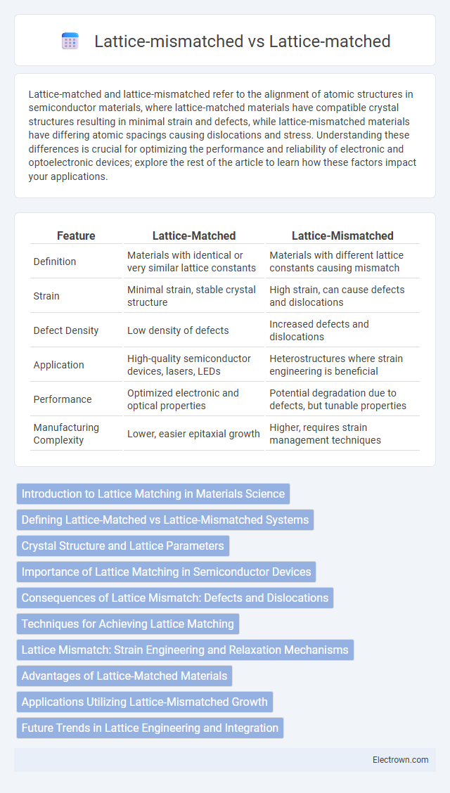
Table of Comparison
| Feature | Lattice-Matched | Lattice-Mismatched |
|---|---|---|
| Definition | Materials with identical or very similar lattice constants | Materials with different lattice constants causing mismatch |
| Strain | Minimal strain, stable crystal structure | High strain, can cause defects and dislocations |
| Defect Density | Low density of defects | Increased defects and dislocations |
| Application | High-quality semiconductor devices, lasers, LEDs | Heterostructures where strain engineering is beneficial |
| Performance | Optimized electronic and optical properties | Potential degradation due to defects, but tunable properties |
| Manufacturing Complexity | Lower, easier epitaxial growth | Higher, requires strain management techniques |
Introduction to Lattice Matching in Materials Science
Lattice matching in materials science involves aligning the crystal lattice parameters of two adjacent materials to minimize strain and defects at their interface. Lattice-matched materials share similar lattice constants, enabling high-quality epitaxial growth and improved electronic or optical properties. Understanding lattice mismatch is crucial for You when designing semiconductor devices, as excessive mismatch can cause dislocations and degrade performance.
Defining Lattice-Matched vs Lattice-Mismatched Systems
Lattice-matched systems feature crystalline materials with identical or nearly identical lattice constants, ensuring minimal strain and high-quality epitaxial growth. Lattice-mismatched systems involve materials whose lattice constants differ significantly, causing strain, dislocations, and defects during layer formation. Understanding the degree of lattice mismatch is critical for optimizing device performance in semiconductor heterostructures and epitaxial film engineering.
Crystal Structure and Lattice Parameters
Crystal structure consistency in lattice-matched materials ensures minimal strain due to closely aligned lattice parameters, typically within a few percent difference, optimizing electronic and optical properties. In contrast, lattice-mismatched materials exhibit significant discrepancies in lattice constants, leading to dislocations and defects that degrade device performance. Managing your semiconductor device's lattice parameters is crucial for achieving high-quality epitaxial growth and reliable crystal integrity.
Importance of Lattice Matching in Semiconductor Devices
Lattice matching is crucial in semiconductor devices as it ensures optimal crystal alignment between different materials, minimizing defects and dislocations that can degrade electronic performance. Semiconductor heterostructures with lattice-matched layers exhibit enhanced carrier mobility, reduced recombination rates, and improved device reliability. Understanding lattice mismatches helps you tailor material interfaces to achieve higher efficiency and longer lifespan in applications such as LEDs, lasers, and high-electron-mobility transistors.
Consequences of Lattice Mismatch: Defects and Dislocations
Lattice mismatch between epitaxial layers causes strain leading to the formation of defects such as misfit dislocations, which degrade crystal quality and electronic properties. These dislocations act as non-radiative recombination centers, reducing carrier mobility and device efficiency in semiconductors. Managing lattice mismatch is critical in advanced materials engineering to minimize defect density and ensure optimal performance of optoelectronic and electronic devices.
Techniques for Achieving Lattice Matching
Techniques for achieving lattice matching include the use of buffer layers composed of intermediate materials that gradually adjust the lattice constant between the substrate and the epitaxial layer, minimizing dislocations. Strain engineering involves carefully controlling layer thickness to accommodate slight lattice mismatches without generating defects, preserving crystal quality. Advanced methods such as metamorphic growth utilize graded compositional layers to create lattice-matched interfaces despite inherent lattice parameter differences.
Lattice Mismatch: Strain Engineering and Relaxation Mechanisms
Lattice mismatch occurs when the crystal lattice parameters of two materials differ, causing strain in epitaxial layers that can be exploited for strain engineering to modify electronic and optical properties in semiconductor devices. Strain relaxation mechanisms, including the formation of misfit dislocations and surface roughening, act to minimize elastic energy but can degrade device performance by introducing defects. Controlling lattice mismatch and understanding relaxation dynamics are critical for optimizing heterostructure quality and functionality in applications like high-electron-mobility transistors and photonic components.
Advantages of Lattice-Matched Materials
Lattice-matched materials offer superior crystal alignment, reducing defects and dislocations in semiconductor devices, which enhances electrical performance and device reliability. This precise atomic arrangement improves carrier mobility and minimizes strain-induced degradation, making your devices more efficient and durable. Such advantages are critical in high-performance applications like LEDs, laser diodes, and high-speed transistors.
Applications Utilizing Lattice-Mismatched Growth
Lattice-mismatched growth enables the fabrication of heterostructure devices such as high-electron-mobility transistors (HEMTs) and quantum cascade lasers by allowing integration of materials with differing lattice constants, thereby tuning electronic and optical properties. This technique is essential for incorporating materials like GaAs on Si substrates, which is critical in photonics and power electronics where cost and scalability matter. Despite the introduction of strain and potential defects, methods like buffer layers and metamorphic growth optimize crystal quality, enhancing device performance in telecommunications and advanced sensing applications.
Future Trends in Lattice Engineering and Integration
Future trends in lattice engineering emphasize the development of advanced epitaxial techniques enabling precise control over lattice matching to reduce defects and enhance device performance. Integration of novel materials such as III-V semiconductors on silicon substrates through lattice-mismatched approaches promises breakthroughs in high-efficiency photonics and power electronics. Emerging strain engineering and buffer layer innovations aim to optimize heteroepitaxy, facilitating scalable production of lattice-mismatched devices with improved reliability and functionality.
Lattice-matched vs Lattice-mismatched Infographic