On-wafer testing provides precise electrical measurements directly on the semiconductor wafer before packaging, enabling early detection of defects and yield improvement, while packaged testing evaluates the final chip performance and functionality after encapsulation. Discover how understanding the differences between on-wafer and packaged testing can optimize your semiconductor quality control process in the rest of this article.
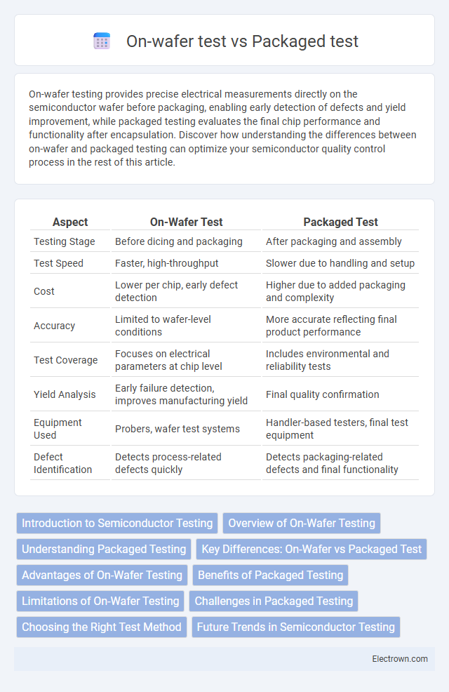
Table of Comparison
| Aspect | On-Wafer Test | Packaged Test |
|---|---|---|
| Testing Stage | Before dicing and packaging | After packaging and assembly |
| Test Speed | Faster, high-throughput | Slower due to handling and setup |
| Cost | Lower per chip, early defect detection | Higher due to added packaging and complexity |
| Accuracy | Limited to wafer-level conditions | More accurate reflecting final product performance |
| Test Coverage | Focuses on electrical parameters at chip level | Includes environmental and reliability tests |
| Yield Analysis | Early failure detection, improves manufacturing yield | Final quality confirmation |
| Equipment Used | Probers, wafer test systems | Handler-based testers, final test equipment |
| Defect Identification | Detects process-related defects quickly | Detects packaging-related defects and final functionality |
Introduction to Semiconductor Testing
Semiconductor testing encompasses critical processes like on-wafer test and packaged test to ensure device functionality and reliability. On-wafer testing assesses individual dies directly on the wafer, enabling early defect detection and yield analysis, while packaged testing evaluates fully enclosed chips under operational conditions for final quality assurance. Your testing strategy should balance these methods to optimize manufacturing efficiency and product performance.
Overview of On-Wafer Testing
On-wafer testing involves evaluating semiconductor devices directly on the wafer before dicing, allowing early detection of defects and process variations. This method provides high-throughput and cost-effective screening by enabling parallel testing of multiple dies under precise probe contact. Your ability to identify issues at the wafer level significantly improves yield and reduces downstream testing requirements compared to packaged tests.
Understanding Packaged Testing
Packaged testing evaluates semiconductor devices after they are enclosed in protective cases, ensuring reliability and functionality in real-world applications. Unlike on-wafer tests that assess bare dies, packaged tests verify electrical performance, thermal management, and mechanical integrity under actual operating conditions. Understanding packaged testing helps you ensure product quality and identify defects that may arise during the packaging process.
Key Differences: On-Wafer vs Packaged Test
On-wafer tests are performed directly on the semiconductor wafer before dicing and packaging, allowing early detection of defects and reducing manufacturing costs by avoiding packaging faulty chips. Packaged tests occur after the wafer is cut and chips are encased, providing a more comprehensive evaluation of final device performance including packaging-induced variations. Key differences lie in the testing stage, with on-wafer tests emphasizing speed and cost-efficiency, while packaged tests emphasize accuracy and reliability verification of the fully assembled integrated circuit.
Advantages of On-Wafer Testing
On-wafer testing allows for early detection of defects directly on the semiconductor wafer, improving yield by identifying faulty dies before packaging. This method reduces costs associated with packaging and testing of non-functional chips, streamlining the production process. Your manufacturing cycle benefits from faster turnaround times and enhanced process control through precise electrical measurements at the wafer level.
Benefits of Packaged Testing
Packaged testing offers enhanced protection of integrated circuits from environmental factors and mechanical damage, ensuring greater reliability and durability during product use. This method facilitates easier handling and compatibility with standard test equipment, leading to improved test accuracy and repeatability. It also enables comprehensive functional testing under end-use conditions, providing a more realistic assessment of device performance before deployment.
Limitations of On-Wafer Testing
On-wafer testing faces limitations such as restricted access to internal device nodes, making it difficult to assess complex circuit functionality fully. The testing environment is more susceptible to noise and parasitic effects due to probe contacts and wafer-level imperfections, which can impact accuracy. Your ability to detect late-stage packaging issues is also compromised because on-wafer tests do not account for stress and variations induced during the packaging process.
Challenges in Packaged Testing
Packaged testing faces challenges such as increased parasitic effects from packaging materials that can distort signal integrity and measurement accuracy compared to on-wafer tests. Thermal dissipation issues and mechanical stresses introduced during packaging can also alter device performance, complicating reliability assessments. Furthermore, the complexity and cost of packaging processes limit the speed and flexibility of testing, making it less efficient than on-wafer characterization for early-stage device evaluation.
Choosing the Right Test Method
Choosing the right test method hinges on balancing accuracy and cost-efficiency: on-wafer tests provide rapid, high-volume screening directly on the semiconductor wafer, enabling early detection of defects before packaging. Packaged tests, performed after encapsulation, offer comprehensive functional verification under real-world conditions but involve higher time and expense. Selecting between on-wafer and packaged testing depends on production scale, required precision, and downstream yield optimization.
Future Trends in Semiconductor Testing
On-wafer testing is expected to advance with the integration of high-frequency probing technology, enabling precise electrical characterization at the wafer level and reducing testing time for next-generation semiconductor devices. Packaged tests will evolve by incorporating more sophisticated built-in self-test (BIST) algorithms and machine learning-based analytics to detect latent defects and improve yield prediction accuracy. The convergence of these trends aims to enhance overall test coverage, minimize costs, and support the manufacturing of smaller, more complex chips used in AI, 5G, and IoT applications.
On-wafer test vs Packaged test Infographic