Gallium Arsenide offers superior electron mobility and higher frequency operation compared to Silicon photonics, making it ideal for high-speed and high-efficiency optoelectronic devices. Explore the rest of the article to understand how Your choice between these materials impacts the performance and applications of photonic technologies.
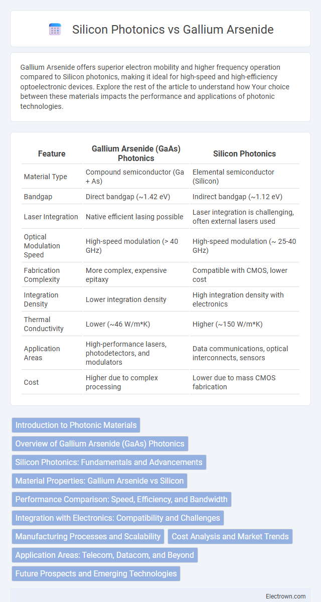
Table of Comparison
| Feature | Gallium Arsenide (GaAs) Photonics | Silicon Photonics |
|---|---|---|
| Material Type | Compound semiconductor (Ga + As) | Elemental semiconductor (Silicon) |
| Bandgap | Direct bandgap (~1.42 eV) | Indirect bandgap (~1.12 eV) |
| Laser Integration | Native efficient lasing possible | Laser integration is challenging, often external lasers used |
| Optical Modulation Speed | High-speed modulation (> 40 GHz) | High-speed modulation (~ 25-40 GHz) |
| Fabrication Complexity | More complex, expensive epitaxy | Compatible with CMOS, lower cost |
| Integration Density | Lower integration density | High integration density with electronics |
| Thermal Conductivity | Lower (~46 W/m*K) | Higher (~150 W/m*K) |
| Application Areas | High-performance lasers, photodetectors, and modulators | Data communications, optical interconnects, sensors |
| Cost | Higher due to complex processing | Lower due to mass CMOS fabrication |
Introduction to Photonic Materials
Gallium Arsenide (GaAs) and Silicon are pivotal materials in photonic technologies, each offering distinct optical and electronic properties essential for high-speed data communication. GaAs exhibits superior electron mobility and direct bandgap characteristics, enabling efficient light emission and high-frequency operation in optoelectronic devices. Silicon photonics leverages mature CMOS fabrication processes and low-cost scalability, although it relies on indirect bandgap materials that necessitate innovative design strategies for effective light manipulation.
Overview of Gallium Arsenide (GaAs) Photonics
Gallium Arsenide (GaAs) photonics offers superior electron mobility and direct bandgap properties, enabling efficient light emission and high-speed optoelectronic devices. GaAs-based components excel in applications requiring high-frequency operation, such as laser diodes and photodetectors, outperforming silicon photonics in speed and wavelength range. Your choice of GaAs photonics can enhance performance in advanced optical communication systems and integrated photonic circuits.
Silicon Photonics: Fundamentals and Advancements
Silicon photonics leverages the mature CMOS fabrication infrastructure to integrate optical components with electronic circuits on a single chip, enabling high-speed data transmission and low-cost mass production. Advancements in silicon photonics include the development of efficient modulators, photodetectors, and wavelength division multiplexing, significantly enhancing bandwidth and energy efficiency for data centers and telecommunications. The compatibility with silicon-based electronics makes silicon photonics a scalable platform for next-generation optical communication and sensing applications.
Material Properties: Gallium Arsenide vs Silicon
Gallium Arsenide (GaAs) offers superior electron mobility and direct bandgap properties, making it highly efficient for high-speed optoelectronic devices compared to Silicon's indirect bandgap and lower electron mobility. GaAs's ability to emit light efficiently enables better integration in photonic applications such as lasers and LEDs, while Silicon's mature fabrication processes and cost-effectiveness favor large-scale electronic-photonic integration. Understanding these material properties helps you choose the right substrate for optimizing performance in photonic circuits and telecommunications.
Performance Comparison: Speed, Efficiency, and Bandwidth
Gallium Arsenide (GaAs) photonics outperforms Silicon photonics in speed due to its higher electron mobility, enabling faster signal processing and reduced latency. Efficiency in GaAs devices is superior, with lower power consumption and better thermal management, making it ideal for high-performance applications. Bandwidth capabilities in GaAs photonics also exceed those of Silicon, supporting wider frequency ranges essential for advanced communication systems and data centers.
Integration with Electronics: Compatibility and Challenges
Gallium Arsenide (GaAs) photonics offers superior electron mobility and direct bandgap properties, enabling high-speed optoelectronic devices but faces integration challenges with silicon-based electronics due to lattice mismatch and thermal expansion differences. Silicon photonics benefits from compatibility with mature CMOS fabrication processes, allowing seamless integration with existing electronic circuits and large-scale production. Your choice depends on balancing GaAs's high-performance optoelectronic advantages against silicon's cost-effective and scalable electronic integration capabilities.
Manufacturing Processes and Scalability
Gallium Arsenide (GaAs) photonics involves more complex and costly manufacturing processes due to its compound semiconductor nature, requiring specialized epitaxial growth techniques such as molecular beam epitaxy (MBE) or metal-organic chemical vapor deposition (MOCVD). Silicon photonics benefits from mature CMOS fabrication infrastructure, enabling high-volume, low-cost scalability and integration with existing silicon-based electronic devices. If your project demands large-scale production and cost efficiency, silicon photonics offers a more scalable manufacturing process compared to GaAs.
Cost Analysis and Market Trends
Gallium Arsenide photonics generally incur higher manufacturing costs compared to Silicon photonics due to expensive raw materials and complex fabrication processes. Silicon photonics dominate the market driven by lower costs, compatibility with existing CMOS technology, and scalability for mass production. Your choice between these technologies should consider cost-effectiveness aligned with current market trends favoring Silicon photonics for telecom and data center applications.
Application Areas: Telecom, Datacom, and Beyond
Gallium Arsenide (GaAs) photonics excels in high-frequency and high-power applications, making it ideal for telecom infrastructure where fast signal processing and low noise are critical. Silicon photonics dominates datacom markets due to its compatibility with CMOS technology, enabling cost-effective, high-density integration for data centers and short-reach optical interconnects. Emerging applications beyond telecom and datacom benefit from GaAs's superior electron mobility for infrared sensors and silicon photonics' scalability for integrated LiDAR and quantum computing systems.
Future Prospects and Emerging Technologies
Gallium Arsenide (GaAs) photonics offers superior electron mobility and direct bandgap properties, making it ideal for high-speed and high-frequency optical applications, while Silicon photonics benefits from mature CMOS integration and cost-effective scalability, driving widespread adoption in data communications. Emerging technologies like hybrid integration of GaAs with Silicon photonics promise enhanced performance by combining GaAs's efficient light emission with Silicon's scalability and low-loss waveguides. Your future photonic systems could leverage these advancements to achieve unprecedented data throughput and energy efficiency in telecommunications and quantum computing.
Gallium Arsenide vs Silicon photonics Infographic