Graphene photodetectors offer ultra-fast response times and a broad spectral range spanning from ultraviolet to terahertz frequencies, outperforming traditional silicon photodetectors known for their limited bandwidth and slower speed. Discover how your choice between graphene and silicon photodetectors can impact the efficiency and performance of optical devices by exploring the detailed comparison ahead.
Table of Comparison
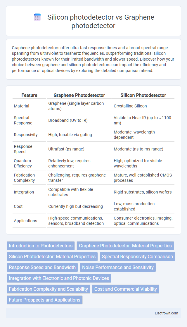
| Feature | Graphene Photodetector | Silicon Photodetector |
|---|---|---|
| Material | Graphene (single layer carbon atoms) | Crystalline Silicon |
| Spectral Response | Broadband (UV to IR) | Visible to Near-IR (up to ~1100 nm) |
| Responsivity | High, tunable via gating | Moderate, wavelength-dependent |
| Response Speed | Ultrafast (ps range) | Moderate (ns to ms range) |
| Quantum Efficiency | Relatively low, requires enhancement | High, optimized for visible wavelengths |
| Fabrication Complexity | Challenging, requires graphene transfer | Mature, well-established CMOS processes |
| Integration | Compatible with flexible substrates | Rigid substrates, silicon wafers |
| Cost | Currently high but decreasing | Low, mass production established |
| Applications | High-speed communications, sensors, broadband detection | Consumer electronics, imaging, optical communications |
Introduction to Photodetectors
Photodetectors are devices that convert light into electrical signals, essential in optical communication, imaging, and sensing technologies. Graphene photodetectors offer ultra-high carrier mobility, broadband absorption, and fast response times, outperforming traditional silicon photodetectors in speed and spectral range. Silicon photodetectors, widely used due to their mature fabrication process and cost-effectiveness, excel in visible to near-infrared detection but face limitations in bandwidth and sensitivity compared to emerging graphene-based devices.
Graphene Photodetector: Material Properties
Graphene photodetectors leverage the exceptional electrical conductivity, high carrier mobility exceeding 200,000 cm2/Vs, and broadband light absorption ranging from ultraviolet to terahertz frequencies inherent to graphene. The two-dimensional atomic structure allows ultrafast photoresponse times in the picosecond regime, enabling high-speed optical detection beyond silicon's limitations. These material properties facilitate enhanced sensitivity and tunable wavelength detection, surpassing traditional silicon photodetectors in applications requiring wide spectral bandwidth and rapid signal processing.
Silicon Photodetector: Material Properties
Silicon photodetectors utilize crystalline silicon known for its excellent semiconductor properties, including a bandgap of 1.12 eV, enabling efficient detection of near-infrared to visible light wavelengths. The material's high electron mobility and mature fabrication technology contribute to its widespread use in optoelectronic applications. However, silicon's limited absorption in the ultraviolet spectrum and recombination losses can restrict performance in certain high-speed or broadband photodetection scenarios.
Spectral Responsivity Comparison
Graphene photodetectors exhibit broadband spectral responsivity ranging from ultraviolet to terahertz frequencies, surpassing the limited spectral range of silicon photodetectors primarily responsive in the visible to near-infrared spectrum (400-1100 nm). Their tunable bandgap and ultrafast carrier mobility enable enhanced sensitivity across a wider wavelength range, making them suitable for diverse optical sensing applications. In contrast, silicon photodetectors offer high responsivity and low noise within their specific range but lack the versatility and extended bandwidth provided by graphene-based devices.
Response Speed and Bandwidth
Graphene photodetectors exhibit significantly higher response speed and broader bandwidth compared to silicon photodetectors due to graphene's exceptional carrier mobility and ultrafast carrier dynamics. Silicon photodetectors are limited by slower carrier recombination rates and narrower absorption spectra, which restrict their operational bandwidth typically under 100 GHz. Graphene devices achieve bandwidths exceeding several hundred GHz, making them ideal for high-speed optical communication and ultrafast photonic applications.
Noise Performance and Sensitivity
Graphene photodetectors exhibit superior noise performance due to their ultrafast carrier mobility and low intrinsic noise levels, enabling high signal-to-noise ratios compared to traditional silicon photodetectors. Their broadband absorption and high responsivity provide enhanced sensitivity, particularly in infrared and terahertz ranges where silicon detectors' sensitivity sharply declines. Optimizing your photodetection system with graphene technology can significantly improve detection accuracy in low-light conditions and high-frequency applications.
Integration with Electronic and Photonic Devices
Graphene photodetectors exhibit superior integration capabilities with both electronic and photonic devices due to their atomic thickness and exceptional electrical conductivity, enabling seamless interfacing with CMOS technology and flexible substrates. Unlike silicon photodetectors, which require complex fabrication processes and often face compatibility challenges with emerging photonic platforms, graphene photodetectors support broadband detection and ultrafast response times, enhancing on-chip optical communication. Their compatibility with various substrate materials and potential for wafer-scale manufacturing make graphene photodetectors highly advantageous for next-generation integrated optoelectronic systems.
Fabrication Complexity and Scalability
Graphene photodetectors offer simpler fabrication processes due to their compatibility with standard CMOS technology and potential for large-area synthesis via chemical vapor deposition (CVD), enabling scalable production. Silicon photodetectors, while benefiting from mature and well-established fabrication infrastructure, face limitations in scalability when miniaturized to nanoscale dimensions due to complex doping and etching steps. The two materials differ significantly in fabrication complexity, with graphene providing a promising pathway for high-throughput, flexible optoelectronic device manufacturing compared to traditional silicon device fabrication.
Cost and Commercial Viability
Graphene photodetectors offer significant advantages in terms of cost due to the material's abundance and scalability of production methods like chemical vapor deposition, reducing manufacturing expenses compared to silicon photodetectors that require complex and energy-intensive fabrication processes. The commercial viability of graphene photodetectors is rapidly increasing as their superior bandwidth, flexibility, and integration capabilities enable new applications in telecommunications and imaging, although silicon photodetectors currently dominate the market due to established supply chains and mature technology. Ongoing advancements in graphene device standardization and large-scale production are expected to further lower costs and enhance commercial adoption, positioning graphene photodetectors as a competitive alternative in next-generation optoelectronics.
Future Prospects and Applications
Graphene photodetectors exhibit superior broadband sensitivity and ultrafast response times compared to silicon photodetectors, positioning them as promising candidates for next-generation optical communication systems and wearable sensors. The exceptional carrier mobility and tunable bandgap of graphene enable integration into flexible electronics, expanding applications in medical imaging and environmental monitoring. As research advances, hybrid graphene-silicon photodetector architectures are expected to enhance device performance, facilitating widespread adoption in telecommunications and IoT technologies.
Graphene photodetector vs Silicon photodetector Infographic