Plasmonic waveguides offer ultra-compact light confinement beyond the diffraction limit by exploiting surface plasmon polaritons, while dielectric waveguides provide low-loss propagation with larger mode sizes suitable for longer distances. Understanding the trade-offs between these waveguide types can help you optimize photonic device performance; explore the rest of the article to learn more.
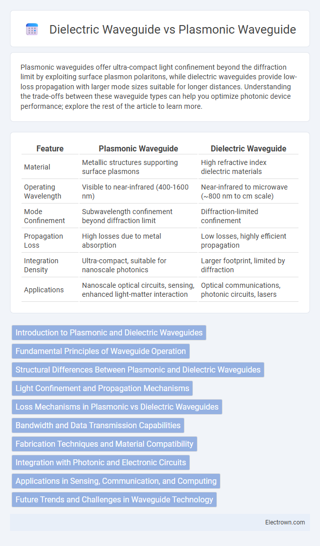
Table of Comparison
| Feature | Plasmonic Waveguide | Dielectric Waveguide |
|---|---|---|
| Material | Metallic structures supporting surface plasmons | High refractive index dielectric materials |
| Operating Wavelength | Visible to near-infrared (400-1600 nm) | Near-infrared to microwave (~800 nm to cm scale) |
| Mode Confinement | Subwavelength confinement beyond diffraction limit | Diffraction-limited confinement |
| Propagation Loss | High losses due to metal absorption | Low losses, highly efficient propagation |
| Integration Density | Ultra-compact, suitable for nanoscale photonics | Larger footprint, limited by diffraction |
| Applications | Nanoscale optical circuits, sensing, enhanced light-matter interaction | Optical communications, photonic circuits, lasers |
Introduction to Plasmonic and Dielectric Waveguides
Plasmonic waveguides utilize surface plasmon polaritons, confining light at metal-dielectric interfaces with nanometer-scale precision, enabling subwavelength optical signal propagation ideal for integrated photonic circuits. Dielectric waveguides rely on total internal reflection within high-refractive-index materials like silicon or silica, offering low-loss light transmission over longer distances suitable for telecommunications. Your choice between plasmonic and dielectric waveguides depends on the application's need for miniaturization versus propagation efficiency.
Fundamental Principles of Waveguide Operation
Plasmonic waveguides operate by coupling light with free electrons at metal-dielectric interfaces, enabling subwavelength light confinement beyond the diffraction limit. Dielectric waveguides rely on total internal reflection within high refractive index materials, guiding light through refractive index contrast between core and cladding. The fundamental difference lies in plasmonic waveguides' ability to confine electromagnetic fields at nanoscale with higher losses, while dielectric waveguides offer lower loss propagation with larger mode sizes.
Structural Differences Between Plasmonic and Dielectric Waveguides
Plasmonic waveguides utilize metal-dielectric interfaces to confine light through surface plasmon polaritons, resulting in subwavelength mode confinement but higher propagation losses. Dielectric waveguides rely on total internal reflection within high-refractive-index materials to guide light with lower losses yet larger mode sizes. Your choice between the two depends on the trade-off between confinement and loss for specific photonic applications.
Light Confinement and Propagation Mechanisms
Plasmonic waveguides achieve subwavelength light confinement by coupling photons with surface plasmons at metal-dielectric interfaces, enabling tight mode confinement beyond the diffraction limit but suffering from higher propagation losses due to metal absorption. Dielectric waveguides confine light through total internal reflection within high-index contrast materials, offering low-loss propagation over longer distances while limited to diffraction-limited mode sizes. Your choice between plasmonic and dielectric waveguides depends on whether ultra-compact confinement or low-loss transmission is prioritized in the application.
Loss Mechanisms in Plasmonic vs Dielectric Waveguides
Plasmonic waveguides experience significant loss primarily due to metal absorption, where free electrons in the metal convert optical energy into heat, limiting propagation length despite strong mode confinement. In contrast, dielectric waveguides exhibit minimal absorption loss, with scattering from surface roughness and material inhomogeneities being the dominant loss mechanisms, enabling longer-distance signal transmission. The trade-off between confinement and loss is crucial, as plasmonic waveguides offer subwavelength confinement at the expense of higher losses compared to low-loss dielectric counterparts.
Bandwidth and Data Transmission Capabilities
Plasmonic waveguides offer ultra-compact confinement of light with bandwidths typically ranging from tens to hundreds of terahertz, enabling high data transmission rates suitable for on-chip optical interconnects. Dielectric waveguides, while larger in size, provide lower propagation losses and support broad bandwidths often exceeding hundreds of terahertz, facilitating long-distance data transmission with minimal signal distortion. The trade-off between plasmonic waveguides' high field confinement and dielectric waveguides' superior low-loss propagation impacts their respective data transmission capabilities in integrated photonic systems.
Fabrication Techniques and Material Compatibility
Plasmonic waveguides are typically fabricated using techniques such as electron beam lithography, focused ion beam milling, and thin-film deposition, which allow for precise nanoscale patterning of metals like gold and silver compatible with CMOS substrates. Dielectric waveguides employ conventional semiconductor fabrication processes including photolithography, chemical vapor deposition, and etching, using materials like silicon, silicon nitride, and silicon dioxide that offer excellent compatibility with integrated photonic circuits. Material compatibility in plasmonic waveguides is limited by metal losses and thermal constraints, whereas dielectric waveguides provide low-loss propagation and greater thermal stability, making them suitable for large-scale photonic integration.
Integration with Photonic and Electronic Circuits
Plasmonic waveguides enable ultra-compact integration with electronic circuits due to their ability to confine light beyond the diffraction limit, providing high field localization at the metal-dielectric interface. Dielectric waveguides, while offering lower propagation losses and compatibility with standard photonic circuit fabrication, require larger footprints for mode confinement. Combining plasmonic waveguides with dielectric components facilitates hybrid photonic-electronic circuits that leverage the high-speed electronic signal processing and efficient optical signal routing.
Applications in Sensing, Communication, and Computing
Plasmonic waveguides enable ultra-compact sensing devices by confining light beyond the diffraction limit, enhancing sensitivity in biochemical and environmental detection. Dielectric waveguides support low-loss signal propagation over long distances, making them ideal for high-speed optical communication networks and integrated photonic circuits. In computing, plasmonic waveguides facilitate ultrafast data processing with nanoscale footprint, while dielectric waveguides provide efficient routing for optical interconnects in photonic chips.
Future Trends and Challenges in Waveguide Technology
Plasmonic waveguides offer unprecedented miniaturization and high field confinement, crucial for future photonic circuits, but face challenges in high propagation losses and fabrication complexities. Dielectric waveguides exhibit low loss and compatibility with existing silicon photonics, making them ideal for large-scale integration, yet their diffraction-limited confinement restricts device scaling. Your innovation in hybrid plasmonic-dielectric structures could overcome current limitations, enabling ultracompact, efficient waveguide systems pivotal for next-generation optical communication and sensing technologies.
plasmonic waveguide vs dielectric waveguide Infographic