Sodium diffusion and ion implantation are two techniques used to introduce dopants into semiconductor materials, with sodium diffusion involving the thermal introduction of sodium atoms into the substrate, while ion implantation uses high-energy ions to precisely embed dopants at controlled depths. Understanding these differences can significantly impact the performance of your semiconductor devices; explore the rest of the article to learn which method suits your application best.
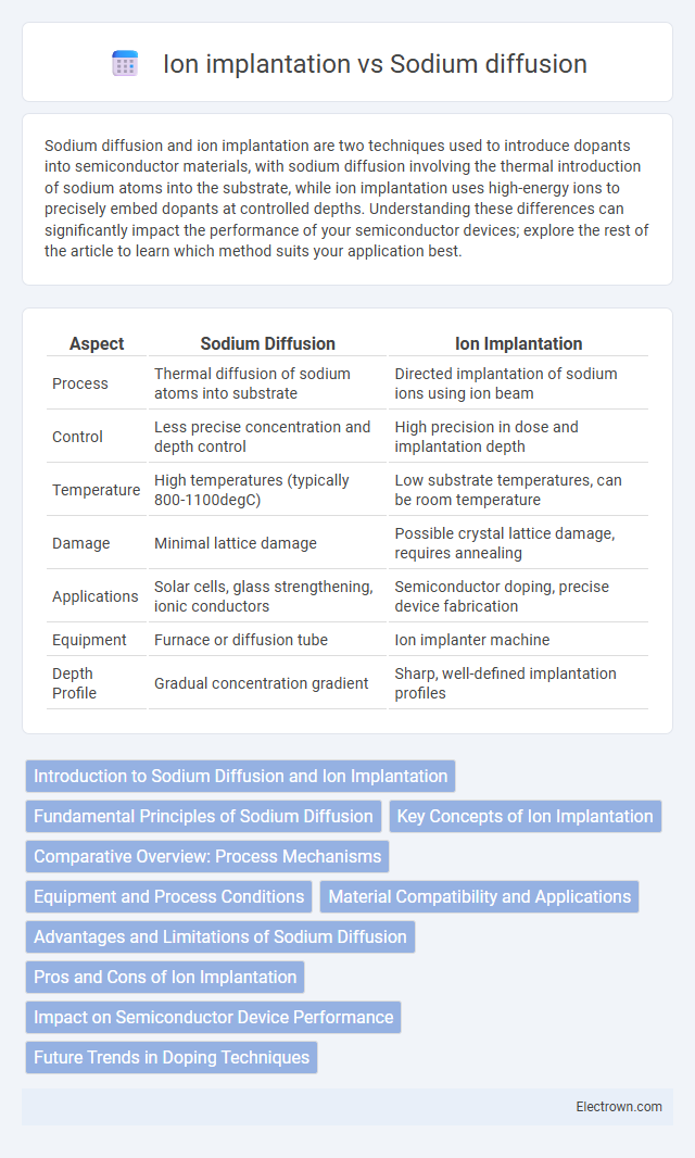
Table of Comparison
| Aspect | Sodium Diffusion | Ion Implantation |
|---|---|---|
| Process | Thermal diffusion of sodium atoms into substrate | Directed implantation of sodium ions using ion beam |
| Control | Less precise concentration and depth control | High precision in dose and implantation depth |
| Temperature | High temperatures (typically 800-1100degC) | Low substrate temperatures, can be room temperature |
| Damage | Minimal lattice damage | Possible crystal lattice damage, requires annealing |
| Applications | Solar cells, glass strengthening, ionic conductors | Semiconductor doping, precise device fabrication |
| Equipment | Furnace or diffusion tube | Ion implanter machine |
| Depth Profile | Gradual concentration gradient | Sharp, well-defined implantation profiles |
Introduction to Sodium Diffusion and Ion Implantation
Sodium diffusion is a thermal process where sodium atoms penetrate a semiconductor substrate, typically silicon, to modify electrical properties and introduce dopants uniformly. Ion implantation involves accelerating sodium ions into the substrate using an electric field, enabling precise control over dopant concentration and depth profiles without requiring high-temperature processes. Both techniques are essential in semiconductor fabrication, with sodium diffusion favoring uniform doping and ion implantation allowing localized, controlled modifications.
Fundamental Principles of Sodium Diffusion
Sodium diffusion involves the movement of sodium ions through a substrate driven by concentration gradients and temperature, following Fick's laws of diffusion. Unlike ion implantation, which forcibly embeds ions into a material using high-energy beams, sodium diffusion relies on thermal energy to enable ions to migrate naturally within the crystal lattice. This process plays a critical role in modifying electrical properties and doping semiconductors by controlling sodium ion concentration and distribution.
Key Concepts of Ion Implantation
Ion implantation involves accelerating ions into a semiconductor substrate to precisely control dopant distribution, differing from sodium diffusion which relies on thermal processes for dopant movement. Key concepts of ion implantation include ion source generation, mass analysis for purity, acceleration voltage determining penetration depth, and dose control to regulate concentration. Your ability to tailor electrical properties and create abrupt doping profiles makes ion implantation essential for modern semiconductor device fabrication.
Comparative Overview: Process Mechanisms
Sodium diffusion involves the thermal migration of sodium ions into a substrate, driven by concentration gradients and typically performed at elevated temperatures ranging from 600degC to 900degC. Ion implantation uses high-energy ion beams to directly embed sodium ions into the substrate lattice, allowing precise control over ion depth and concentration profiles without requiring high-temperature processing. While sodium diffusion relies on solid-state ionic mobility and time-dependent thermal activation, ion implantation uses kinetic energy to overcome lattice barriers, resulting in distinct damage or defect creation within the crystal structure.
Equipment and Process Conditions
Sodium diffusion utilizes tubular or quartz diffusion furnaces operating at temperatures between 900degC and 1100degC, allowing controlled sodium vapor to diffuse into semiconductor substrates. Ion implantation requires high-vacuum ion implanters equipped with ion sources, mass analyzers, and acceleration systems to precisely inject sodium ions at energies ranging from 10 keV to 100 keV under ultra-clean conditions. Diffusion demands prolonged thermal exposure for dopant activation and redistribution, whereas ion implantation offers accurate dose and depth control with subsequent annealing needed to repair crystal damage.
Material Compatibility and Applications
Sodium diffusion is primarily compatible with glass and certain oxide materials, making it ideal for modifying surface properties in applications such as glass strengthening and semiconductor passivation. Ion implantation offers broader material compatibility, including metals, semiconductors, and insulators, enabling precise doping and alteration of electrical, optical, and mechanical properties in microelectronics and advanced materials engineering. While sodium diffusion is limited in application due to material and temperature constraints, ion implantation's versatility supports high-precision fabrication processes in integrated circuit manufacturing and nanotechnology.
Advantages and Limitations of Sodium Diffusion
Sodium diffusion offers a cost-effective and straightforward technique for doping silicon wafers, enabling uniform surface concentration and deep junction formation essential for solar cell manufacturing. However, limitations include poor depth control compared to ion implantation, higher thermal budget requirements, and difficulty achieving precise spatial doping profiles. Despite these challenges, sodium diffusion remains advantageous for large-scale photovoltaic applications due to scalability and equipment simplicity.
Pros and Cons of Ion Implantation
Ion implantation offers precise control over dopant concentration and depth profiles, enabling tailored electrical properties essential for advanced semiconductor device fabrication. The process causes minimal substrate damage compared to diffusion methods and allows low-temperature processing, which preserves device integrity and reduces unwanted diffusion phenomena. However, ion implantation equipment is costly, implantation-induced lattice damage requires post-implantation annealing, and contamination risks can affect device performance if proper protocols are not followed.
Impact on Semiconductor Device Performance
Sodium diffusion introduces mobile ions that can cause threshold voltage shifts and increased leakage currents in semiconductor devices, deteriorating long-term stability. Ion implantation offers precise control over dopant concentration and distribution, enhancing device performance by reducing defects and enabling shallow junctions critical for scaling. Compared to sodium diffusion, ion implantation minimizes contamination and improves the reproducibility of electrical characteristics in advanced integrated circuits.
Future Trends in Doping Techniques
Emerging trends in doping techniques emphasize precision and scalability, with sodium diffusion offering cost-effective, high-throughput options for large-area substrates, while ion implantation provides superior control over dopant profiles essential for nanoscale devices. Advanced femtosecond laser-assisted ion implantation is gaining traction to enhance dopant activation and minimize lattice damage. Integration of machine learning for process optimization and real-time monitoring is driving improved consistency and performance in both sodium diffusion and ion implantation methods.
Sodium diffusion vs ion implantation Infographic