Switching loss occurs when a transistor transitions between on and off states, generating heat and reducing efficiency, whereas conduction loss happens when current flows through a device's resistance during its on state. Understanding the differences between switching loss and conduction loss will help you optimize your power electronics design; explore the article to learn how to minimize these losses effectively.
Table of Comparison
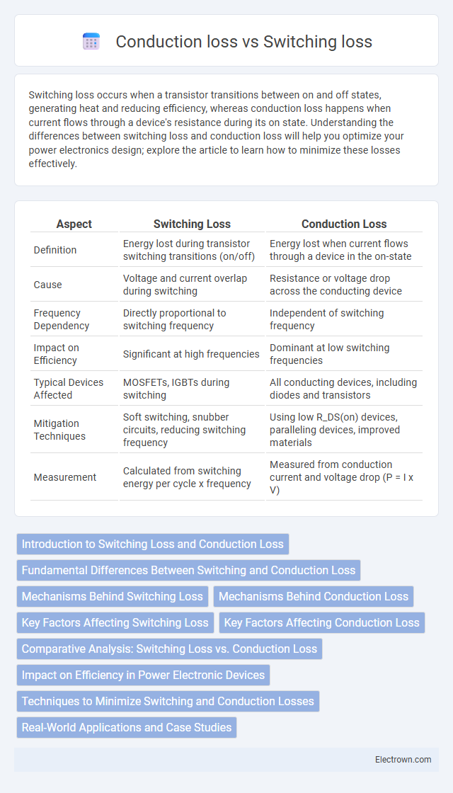
| Aspect | Switching Loss | Conduction Loss |
|---|---|---|
| Definition | Energy lost during transistor switching transitions (on/off) | Energy lost when current flows through a device in the on-state |
| Cause | Voltage and current overlap during switching | Resistance or voltage drop across the conducting device |
| Frequency Dependency | Directly proportional to switching frequency | Independent of switching frequency |
| Impact on Efficiency | Significant at high frequencies | Dominant at low switching frequencies |
| Typical Devices Affected | MOSFETs, IGBTs during switching | All conducting devices, including diodes and transistors |
| Mitigation Techniques | Soft switching, snubber circuits, reducing switching frequency | Using low R_DS(on) devices, paralleling devices, improved materials |
| Measurement | Calculated from switching energy per cycle x frequency | Measured from conduction current and voltage drop (P = I x V) |
Introduction to Switching Loss and Conduction Loss
Switching loss occurs during the transition periods when a power device changes states from on to off or vice versa, causing energy dissipation due to non-instantaneous switching. Conduction loss happens when the device is fully on, resulting from the inherent resistance or voltage drop across the component during current flow. Understanding the balance between switching loss and conduction loss is crucial for optimizing the efficiency of power electronics in your design.
Fundamental Differences Between Switching and Conduction Loss
Switching loss occurs during the transition periods when a semiconductor device changes states between on and off, causing energy dissipation due to voltage and current overlap. Conduction loss happens when the device is fully on, resulting from its inherent resistance causing continuous power dissipation. Understanding the fundamental differences between switching and conduction loss helps you optimize electronic circuit efficiency by balancing device selection and switching frequency.
Mechanisms Behind Switching Loss
Switching loss occurs due to the energy dissipated during the transition of semiconductor devices between on and off states, primarily caused by overlap between voltage and current in the device. The loss mechanisms involve charging and discharging of parasitic capacitances and non-ideal switching speeds leading to time intervals where both voltage and current are significant. These losses increase with switching frequency, impacting the efficiency of power converters and requiring careful device and circuit design to minimize energy dissipation during transitions.
Mechanisms Behind Conduction Loss
Conduction loss in power electronics occurs due to the resistance encountered when current flows through semiconductor devices, primarily resulting in heat generation during the device's ON state. This loss is influenced by factors such as the device's on-resistance (R_DS(on)) and the magnitude of the current passing through it, directly affecting efficiency. Unlike switching losses, conduction losses increase proportionally with load current and are a critical consideration in the thermal management and design of MOSFETs and IGBTs.
Key Factors Affecting Switching Loss
Switching loss in power electronics primarily depends on switching frequency, voltage, and current transitions, which cause energy dissipation during device turn-on and turn-off events. The key factors affecting switching loss include the transistor's switching speed, gate charge, and the overlap between voltage and current waveforms during switching intervals. Reducing switching loss improves efficiency and thermal management, directly benefiting your device's performance and reliability.
Key Factors Affecting Conduction Loss
Conduction loss primarily depends on the device's on-resistance (R_DS(on)) and the current flowing through it, with higher currents increasing power dissipation linearly. Thermal management and device packaging significantly influence conduction loss by impacting the junction temperature, which in turn affects R_DS(on) values. You can reduce conduction loss by selecting MOSFETs with lower R_DS(on) and ensuring efficient heat sinking to maintain optimal operating temperatures.
Comparative Analysis: Switching Loss vs. Conduction Loss
Switching loss occurs during the transition of power devices between on and off states, heavily influenced by switching frequency and voltage stress, while conduction loss arises from the resistance in the device when it is in the on state, directly related to current flow and on-resistance (R_DS(on)). In high-frequency applications, switching losses dominate due to rapid switching transitions, whereas conduction losses become more significant at lower frequencies with sustained current flow. Efficient power electronics design requires balancing these losses by selecting devices with optimized R_DS(on) and switching characteristics to minimize total energy dissipation.
Impact on Efficiency in Power Electronic Devices
Switching loss and conduction loss significantly affect the efficiency of power electronic devices, with switching loss increasing during high-frequency operations due to energy dissipated during transistor transitions. Conduction loss arises from the resistance of the semiconductor when current flows, leading to continuous power dissipation proportional to current magnitude. Minimizing switching loss through soft-switching techniques and reducing conduction loss by using low-resistance materials enhances overall device efficiency and thermal management.
Techniques to Minimize Switching and Conduction Losses
Techniques to minimize switching losses include soft-switching methods such as zero-voltage switching (ZVS) and zero-current switching (ZCS), which reduce voltage or current overlap during transistor transitions. For conduction losses, using low-resistance materials like silicon carbide (SiC) or gallium nitride (GaN) devices improves efficiency by lowering on-state resistance (R_DS(on)). You can further enhance overall power efficiency by optimizing gate drive circuits and employing synchronous rectification to reduce both switching and conduction losses in power electronics systems.
Real-World Applications and Case Studies
Switching loss and conduction loss critically influence the efficiency of power electronics in applications like electric vehicles and renewable energy systems, where minimizing thermal stress and improving energy conversion are paramount. Case studies in inverter design for photovoltaic systems reveal that reducing switching loss through advanced semiconductor materials, such as SiC and GaN, significantly enhances overall system performance and reliability. Real-world implementations demonstrate that optimizing conduction loss by refining device geometry and employing low-resistance materials can lead to substantial improvements in power density and operational lifespan.
Switching loss vs Conduction loss Infographic