Off-state breakdown occurs when a device unintentionally conducts current under high voltage while in the non-conducting state, risking damage or failure. Understanding the difference between off-state and on-state breakdown is crucial for optimizing your device's performance and reliability; explore the full article to learn more.
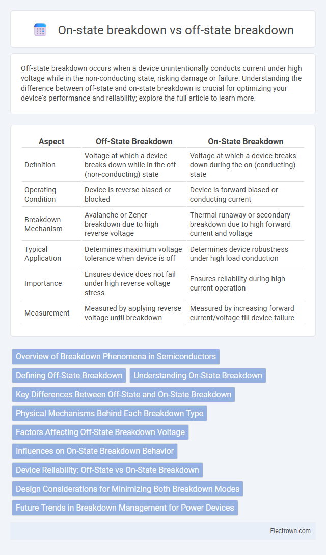
Table of Comparison
| Aspect | Off-State Breakdown | On-State Breakdown |
|---|---|---|
| Definition | Voltage at which a device breaks down while in the off (non-conducting) state | Voltage at which a device breaks down during the on (conducting) state |
| Operating Condition | Device is reverse biased or blocked | Device is forward biased or conducting current |
| Breakdown Mechanism | Avalanche or Zener breakdown due to high reverse voltage | Thermal runaway or secondary breakdown due to high forward current and voltage |
| Typical Application | Determines maximum voltage tolerance when device is off | Determines device robustness under high load conduction |
| Importance | Ensures device does not fail under high reverse voltage stress | Ensures reliability during high current operation |
| Measurement | Measured by applying reverse voltage until breakdown | Measured by increasing forward current/voltage till device failure |
Overview of Breakdown Phenomena in Semiconductors
Off-state breakdown in semiconductors occurs when a high reverse voltage causes avalanche or Zener breakdown, leading to uncontrolled current flow and potential device failure. On-state breakdown happens during forward conduction when excessive current density and joule heating induce thermal runaway or electromigration, damaging the device structure. Understanding these breakdown mechanisms is critical for optimizing device reliability and designing robust power semiconductor components.
Defining Off-State Breakdown
Off-state breakdown occurs when a semiconductor device such as a transistor or diode fails to withstand voltage while it is supposed to be non-conductive, leading to unintended current flow. This phenomenon is critical in power electronics, where maintaining device insulation during off-state ensures circuit reliability and safety. Understanding your device's off-state breakdown voltage helps prevent damage during high-voltage stresses when the switch is turned off.
Understanding On-State Breakdown
Understanding on-state breakdown involves analyzing the voltage at which a semiconductor device, such as a MOSFET or diode, fails to maintain its conductive state under forward bias conditions. This phenomenon occurs when the device current reaches a critical threshold, causing an irreversible increase in conductivity and potential damage to the device structure. Unlike off-state breakdown, which happens during reverse bias, on-state breakdown focuses on sustaining device integrity while operating under load and high current flow.
Key Differences Between Off-State and On-State Breakdown
Off-state breakdown occurs when a device blocks voltage beyond its rated limit without conducting current, while on-state breakdown happens when the device is conducting current and fails due to excessive voltage or current. The key difference lies in the condition of the device: off-state breakdown represents the maximum voltage the device can withstand in its non-conducting state, whereas on-state breakdown relates to failure during conduction under high stress. Understanding these differences ensures your electronic components operate safely within their voltage and current ratings.
Physical Mechanisms Behind Each Breakdown Type
Off-state breakdown occurs when a high reverse voltage causes avalanche multiplication or tunneling effects in the semiconductor depletion region, leading to a sudden increase in leakage current. On-state breakdown involves excessive current densities and joule heating, which result in thermal runaway and device failure due to localized hotspots. Understanding these physical mechanisms helps you design more robust semiconductor devices capable of withstanding both voltage and current stresses.
Factors Affecting Off-State Breakdown Voltage
Off-state breakdown voltage primarily depends on factors such as doping concentration, semiconductor material properties, and device geometry, including junction depth and spacing. Higher doping levels typically reduce off-state breakdown voltage by increasing electric field intensity, while wider junction spacing and materials with higher critical electric field strength enhance it. Additionally, surface conditions and temperature variations influence the off-state breakdown voltage by affecting carrier mobility and trap states.
Influences on On-State Breakdown Behavior
On-state breakdown behavior in semiconductors is primarily influenced by factors such as device material quality, charge carrier mobility, and temperature effects, which alter the conduction pathways and electric field distribution. The presence of defects, impurities, and interface states can exacerbate localized heating and accelerate degradation, leading to a lower on-state breakdown voltage. Additionally, device geometry and doping concentration critically impact the uniformity of current flow and the onset of avalanche breakdown during the on-state operation.
Device Reliability: Off-State vs On-State Breakdown
Off-state breakdown occurs when a device fails to block voltage in its non-conducting state, causing leakage or catastrophic damage, while on-state breakdown refers to failure during conduction due to excessive current or thermal stress. Device reliability hinges on the robustness of both breakdown mechanisms, as off-state breakdown impacts long-term insulation integrity and on-state breakdown affects operational endurance under high load. Optimizing semiconductor materials and device architecture enhances tolerance to off-state voltage stresses and on-state current stresses, ensuring durable performance in power electronics.
Design Considerations for Minimizing Both Breakdown Modes
Minimizing off-state breakdown requires careful design of the device's depletion region and doping profile to prevent avalanche multiplication under high reverse bias, ensuring a high breakdown voltage without excessive leakage. On-state breakdown necessitates optimizing channel length and gate oxide quality to avoid hot carrier injection and punch-through, maintaining device reliability under high forward current. Balancing these considerations involves trade-offs in doping concentration, gate geometry, and material quality to achieve robust performance across both operating states.
Future Trends in Breakdown Management for Power Devices
Future trends in breakdown management for power devices emphasize advanced material engineering and novel device architectures to enhance off-state and on-state breakdown voltage performance. Wide bandgap semiconductors like SiC and GaN demonstrate superior off-state breakdown characteristics, enabling higher voltage blocking capabilities and reduced leakage currents in power transistors. Integration of real-time monitoring and adaptive bias control methods offers improved reliability by dynamically managing on-state breakdown stress during high-current operation.
Off-state breakdown vs on-state breakdown Infographic