Surface passivation focuses on protecting and stabilizing the outer layer of a material to prevent oxidation and contamination, while bulk passivation targets the interior atoms to reduce defects and improve the material's overall electrical properties. Understanding these differences can help you choose the right method for enhancing the performance and durability of semiconductor devices; read on to explore the detailed benefits and applications of each technique.
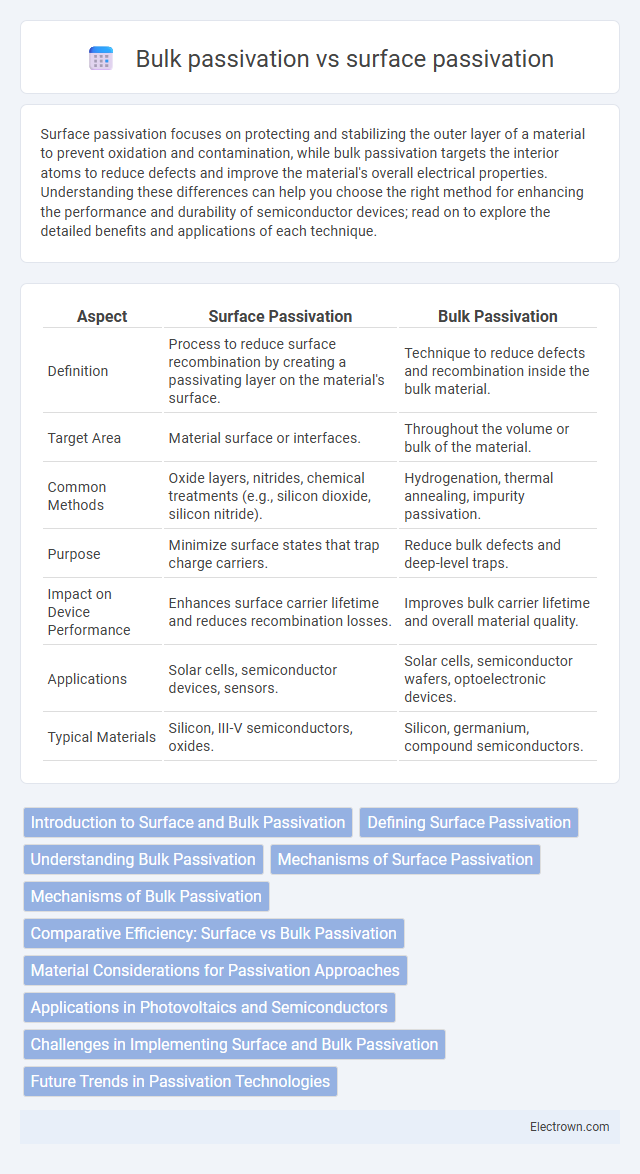
Table of Comparison
| Aspect | Surface Passivation | Bulk Passivation |
|---|---|---|
| Definition | Process to reduce surface recombination by creating a passivating layer on the material's surface. | Technique to reduce defects and recombination inside the bulk material. |
| Target Area | Material surface or interfaces. | Throughout the volume or bulk of the material. |
| Common Methods | Oxide layers, nitrides, chemical treatments (e.g., silicon dioxide, silicon nitride). | Hydrogenation, thermal annealing, impurity passivation. |
| Purpose | Minimize surface states that trap charge carriers. | Reduce bulk defects and deep-level traps. |
| Impact on Device Performance | Enhances surface carrier lifetime and reduces recombination losses. | Improves bulk carrier lifetime and overall material quality. |
| Applications | Solar cells, semiconductor devices, sensors. | Solar cells, semiconductor wafers, optoelectronic devices. |
| Typical Materials | Silicon, III-V semiconductors, oxides. | Silicon, germanium, compound semiconductors. |
Introduction to Surface and Bulk Passivation
Surface passivation involves treating the outermost layer of a semiconductor to reduce surface defects and minimize recombination of charge carriers. Bulk passivation focuses on improving the internal quality of the semiconductor material by neutralizing defects and impurities within the bulk crystal structure. Both techniques aim to enhance the efficiency and longevity of devices such as solar cells and semiconductor lasers.
Defining Surface Passivation
Surface passivation involves the treatment of the outer layer of a semiconductor material to reduce surface defect states that act as recombination centers for charge carriers, thereby enhancing electronic device performance. This process typically includes applying thin dielectric films such as silicon nitride or silicon oxide to chemically stabilize the surface and prevent contamination or oxidation. By contrast, bulk passivation targets the reduction of defects within the material's interior, focusing on improving the semiconductor's inherent crystallographic quality and carrier lifetime.
Understanding Bulk Passivation
Bulk passivation involves neutralizing defects within the interior of a semiconductor material to improve its electrical properties and enhance device performance. This process reduces recombination losses by stabilizing charge carriers throughout the bulk, leading to higher efficiency in solar cells and electronic components. Understanding bulk passivation helps optimize the longevity and reliability of your semiconductor devices by minimizing deep-level traps and intrinsic defects.
Mechanisms of Surface Passivation
Surface passivation involves creating a thin insulating layer or chemical treatment on the semiconductor surface to reduce dangling bonds and trap states that cause recombination of charge carriers. Mechanisms of surface passivation include chemical passivation, where atoms saturate surface bonds, and field-effect passivation, which uses charges in the passivation layer to repel minority carriers from the surface. Comparing to bulk passivation, surface passivation directly targets interface defects, enhancing device performance by minimizing surface recombination velocities.
Mechanisms of Bulk Passivation
Bulk passivation involves the reduction of electrically active defects within the interior of a semiconductor material, improving carrier lifetime and material quality by neutralizing recombination centers. This process typically uses hydrogenation or other chemical treatments to passivate dangling bonds and impurities embedded deep in the bulk material. Understanding these mechanisms optimizes Your semiconductor device performance by minimizing bulk recombination losses.
Comparative Efficiency: Surface vs Bulk Passivation
Surface passivation targets the reduction of recombination sites on the outermost layer of a semiconductor, significantly improving charge carrier lifetime at the interface and boosting device efficiency. Bulk passivation, on the other hand, addresses defects within the interior material, leading to enhanced overall material quality and minority carrier diffusion length. Your photovoltaic device's performance hinges on balancing both surface and bulk passivation to minimize recombination losses and maximize energy conversion efficiency.
Material Considerations for Passivation Approaches
Material considerations for surface passivation focus on minimizing defects and recombination at the interface of semiconductors like silicon or GaAs through thin oxide layers, nitrides, or organic coatings that preserve electronic properties. Bulk passivation involves introducing hydrogen or other passivating species within the wafer substrate to neutralize deep-level traps and impurities, enhancing carrier lifetime in materials such as crystalline silicon or perovskites. Your choice depends on the semiconductor type and device application, as surface passivation targets interface states while bulk passivation improves the intrinsic quality of the material.
Applications in Photovoltaics and Semiconductors
Surface passivation enhances photovoltaic efficiency by reducing surface recombination velocity, thereby increasing carrier lifetime at the semiconductor interface. Bulk passivation mitigates defects within the semiconductor material, improving charge carrier mobility and reducing bulk recombination in devices like silicon solar cells and photodetectors. Both methods are critical in semiconductor fabrication to optimize electronic properties and boost overall device performance.
Challenges in Implementing Surface and Bulk Passivation
Implementing surface passivation poses challenges such as controlling interface states and achieving uniform coverage to minimize recombination losses, which is critical for devices like solar cells. Bulk passivation requires precise doping and defect management within the semiconductor material to enhance carrier lifetime without compromising conductivity. Your success depends on balancing these approaches to optimize overall device performance while mitigating material and process complexities.
Future Trends in Passivation Technologies
Emerging trends in passivation technologies emphasize advanced surface passivation techniques, such as atomic layer deposition and organic-inorganic hybrid coatings, which enhance interface stability and reduce surface recombination velocity significantly. Bulk passivation developments focus on defect engineering and hydrogenation methods to mitigate bulk trap states, improving carrier lifetime and overall device performance. Integration of machine learning for process optimization and development of self-healing passivation layers represent future milestones driving higher efficiency in semiconductor and photovoltaic applications.
Surface passivation vs bulk passivation Infographic