Latch-up occurs when a parasitic structure within a CMOS device creates a low-resistance path, causing device failure, while punch-through happens when the depletion regions of a transistor's junctions merge, leading to uncontrollable current flow and device breakdown. Understanding these mechanisms helps you prevent circuit malfunctions and improve semiconductor device reliability; explore the rest of the article to learn detailed differences and prevention techniques.
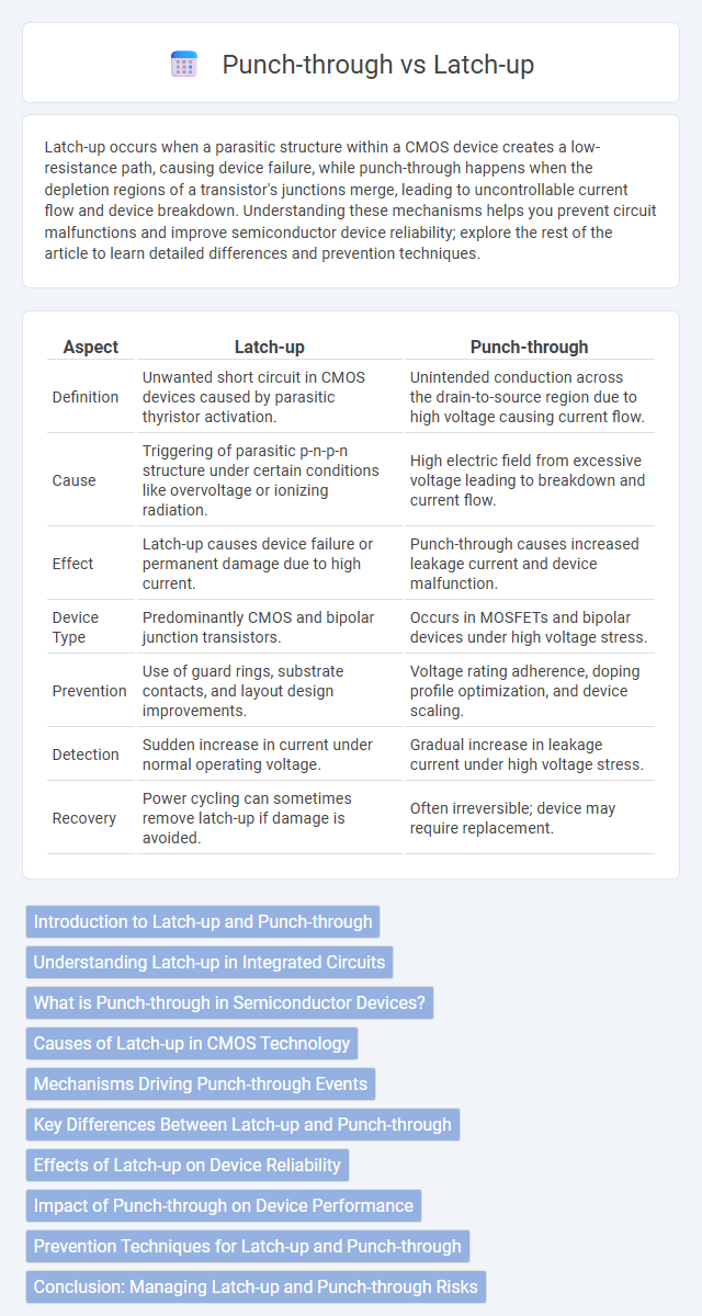
Table of Comparison
| Aspect | Latch-up | Punch-through |
|---|---|---|
| Definition | Unwanted short circuit in CMOS devices caused by parasitic thyristor activation. | Unintended conduction across the drain-to-source region due to high voltage causing current flow. |
| Cause | Triggering of parasitic p-n-p-n structure under certain conditions like overvoltage or ionizing radiation. | High electric field from excessive voltage leading to breakdown and current flow. |
| Effect | Latch-up causes device failure or permanent damage due to high current. | Punch-through causes increased leakage current and device malfunction. |
| Device Type | Predominantly CMOS and bipolar junction transistors. | Occurs in MOSFETs and bipolar devices under high voltage stress. |
| Prevention | Use of guard rings, substrate contacts, and layout design improvements. | Voltage rating adherence, doping profile optimization, and device scaling. |
| Detection | Sudden increase in current under normal operating voltage. | Gradual increase in leakage current under high voltage stress. |
| Recovery | Power cycling can sometimes remove latch-up if damage is avoided. | Often irreversible; device may require replacement. |
Introduction to Latch-up and Punch-through
Latch-up occurs in CMOS devices when a parasitic thyristor structure is inadvertently triggered, causing a low-impedance path between power and ground that can lead to device failure. Punch-through happens when the depletion regions of adjacent junctions within a transistor extend and merge under high voltage, allowing current to flow uncontrollably between source and drain. Both phenomena jeopardize device reliability but differ fundamentally in their mechanisms and affected device structures.
Understanding Latch-up in Integrated Circuits
Latch-up in integrated circuits occurs when parasitic thyristor structures become inadvertently triggered, causing a low-impedance path between power supply rails that leads to high current and potential device failure. Punch-through is a distinct phenomenon where increased voltage causes the depletion regions in a transistor to merge, resulting in unintended current flow and device breakdown. Understanding latch-up helps you design ICs with proper substrate resistivity and guard rings to prevent these destructive conditions.
What is Punch-through in Semiconductor Devices?
Punch-through in semiconductor devices occurs when the depletion region of the drain extends into the channel beyond the control of the gate, causing a sharp increase in leakage current. This phenomenon typically happens at high drain voltages, leading to loss of device control and possible failure. You can prevent punch-through by designing devices with appropriate channel length and doping profiles to maintain proper electrostatic control.
Causes of Latch-up in CMOS Technology
Latch-up in CMOS technology is primarily caused by the inadvertent creation of a low-impedance path between the power supply and ground due to parasitic silicon-controlled rectifier (SCR) structures within the integrated circuit. Factors such as high voltage transients, ionizing radiation, or improper layout design can trigger these parasitic thyristors, leading to excessive current flow and potential device failure. The presence of closely spaced p-n-p and n-p-n transistors in the CMOS substrate forms the basis for latch-up susceptibility.
Mechanisms Driving Punch-through Events
Punch-through events occur when the depletion regions of adjacent semiconductor junctions extend and merge under high voltage stress, allowing current to flow uncontrollably between them. This mechanism is driven primarily by high electric fields that reduce the potential barrier, causing a sudden increase in carrier injection and resulting in device malfunction or breakdown. Unlike latch-up, which involves parasitic thyristor action, punch-through is dominated by direct punch-through of the depletion regions leading to device failure.
Key Differences Between Latch-up and Punch-through
Latch-up occurs when a parasitic thyristor within an integrated circuit triggers, causing a high current flow that can permanently damage the device, whereas punch-through happens when a high voltage causes the depletion regions of a transistor's source and drain to merge, leading to uncontrolled current flow. Latch-up is typically triggered by transient spikes or ionizing radiation, while punch-through is a breakdown phenomenon related to device geometry and doping profiles under extreme voltage stress. Understanding these differences helps you design more reliable semiconductor devices by optimizing circuit layout and voltage margins.
Effects of Latch-up on Device Reliability
Latch-up causes a sudden, high current flow that can permanently damage semiconductor devices by overheating and degrading the junctions, leading to device failure. This phenomenon significantly reduces device reliability by inducing permanent latch state conditions, which may require circuit-level resets or even physical intervention. Your circuits must incorporate protective measures like guard rings and proper layout techniques to mitigate latch-up and maintain long-term device stability.
Impact of Punch-through on Device Performance
Punch-through in semiconductor devices causes a significant increase in leakage current, leading to reduced device reliability and performance degradation. This phenomenon occurs when the depletion regions of the source and drain extend and merge, allowing current to bypass the channel, which adversely affects the switching behavior and power efficiency. Understanding punch-through is crucial for optimizing your device design to maintain stable operation and prevent premature failure.
Prevention Techniques for Latch-up and Punch-through
Prevention techniques for latch-up include the use of guard rings, proper substrate doping, and optimized well contacts to isolate parasitic transistors, significantly reducing the risk of unintended thyristor formation. For punch-through prevention, designers implement thicker epitaxial layers, optimized channel doping profiles, and shallow junctions to control the electric field distribution and improve breakdown voltage. Both methods rely on precise semiconductor fabrication and layout strategies to maintain device reliability and performance under high-voltage stress.
Conclusion: Managing Latch-up and Punch-through Risks
Effective management of latch-up and punch-through risks in semiconductor devices hinges on optimizing device structure and process parameters to enhance junction integrity and reduce parasitic current paths. Implementing guard rings, adjusting doping concentrations, and utilizing silicon-on-insulator (SOI) technology are critical techniques for mitigating latch-up susceptibility and preventing punch-through breakdown. Continuous monitoring of device operating conditions and maintaining robust design margins ensure reliable performance and longevity in integrated circuits.
Latch-up vs punch-through Infographic