Strained silicon enhances electron mobility by stretching the silicon lattice, resulting in faster transistor performance compared to bulk silicon's regular lattice structure. Explore the rest of the article to understand how this technology impacts your device's speed and efficiency.
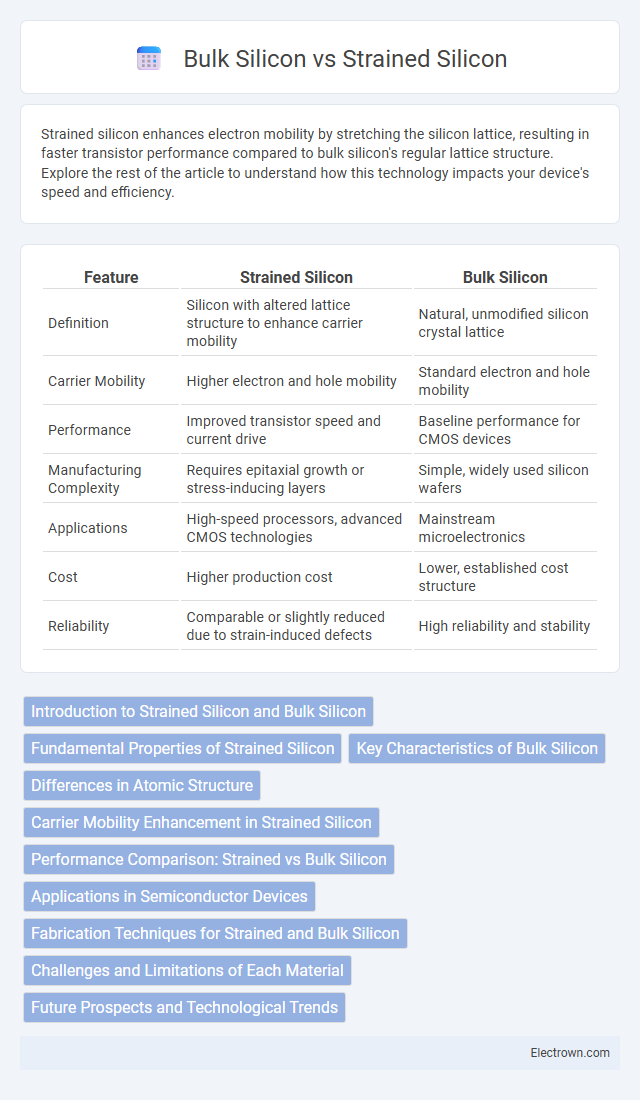
Table of Comparison
| Feature | Strained Silicon | Bulk Silicon |
|---|---|---|
| Definition | Silicon with altered lattice structure to enhance carrier mobility | Natural, unmodified silicon crystal lattice |
| Carrier Mobility | Higher electron and hole mobility | Standard electron and hole mobility |
| Performance | Improved transistor speed and current drive | Baseline performance for CMOS devices |
| Manufacturing Complexity | Requires epitaxial growth or stress-inducing layers | Simple, widely used silicon wafers |
| Applications | High-speed processors, advanced CMOS technologies | Mainstream microelectronics |
| Cost | Higher production cost | Lower, established cost structure |
| Reliability | Comparable or slightly reduced due to strain-induced defects | High reliability and stability |
Introduction to Strained Silicon and Bulk Silicon
Strained silicon enhances electron mobility by applying mechanical stress to the silicon lattice, improving transistor speed and performance compared to bulk silicon. Bulk silicon, the traditional semiconductor material, maintains an unaltered crystal structure, resulting in standard electrical properties. You can significantly boost device efficiency by choosing strained silicon for advanced semiconductor applications.
Fundamental Properties of Strained Silicon
Strained silicon exhibits enhanced electron mobility compared to bulk silicon due to tensile strain altering its crystal lattice structure, which reduces effective electron mass and scattering rates. This modification in band structure leads to increased carrier velocity and improved transistor performance in CMOS technology. Mechanical strain engineering in strained silicon is pivotal for achieving higher drive currents and faster switching speeds in modern semiconductor devices.
Key Characteristics of Bulk Silicon
Bulk silicon features a crystalline structure with uniform lattice spacing, which provides stable electrical properties and reliability in semiconductor devices. Its intrinsic carrier mobility and bandgap are well-characterized, making it a standard material for conventional integrated circuits. You can expect consistent performance in terms of electron flow and thermal conductivity, critical for general-purpose silicon-based electronics.
Differences in Atomic Structure
Strained silicon features a lattice structure stretched or compressed to alter atomic spacing, enhancing electron mobility compared to bulk silicon with its regular, unstrained crystal lattice. The atomic distortion in strained silicon reduces scattering and improves carrier velocity, leading to better device performance. Bulk silicon maintains a natural atomic arrangement, which limits electron flow and switching speeds in semiconductor devices.
Carrier Mobility Enhancement in Strained Silicon
Strained silicon significantly improves carrier mobility compared to bulk silicon by altering the silicon lattice structure, resulting in reduced electron and hole scattering. This enhancement boosts transistor performance and increases drive current in CMOS devices, making strained silicon a preferred choice for advanced semiconductor manufacturing. Your circuits benefit from faster switching speeds and lower power consumption due to this superior carrier transport efficiency.
Performance Comparison: Strained vs Bulk Silicon
Strained silicon significantly enhances carrier mobility compared to bulk silicon, resulting in faster transistor switching speeds and improved overall device performance. This increased electron and hole mobility in strained silicon reduces power consumption and allows for higher drive currents in integrated circuits. Your choice of strained silicon over bulk silicon can lead to more efficient, high-performance semiconductor devices that meet the demands of advanced computing applications.
Applications in Semiconductor Devices
Strained silicon enhances electron mobility, leading to faster transistors in high-performance microprocessors and advanced integrated circuits compared to bulk silicon. It is widely used in Metal-Oxide-Semiconductor Field-Effect Transistors (MOSFETs) for improved switching speed and reduced power consumption in mobile devices and data centers. Bulk silicon remains prevalent in cost-sensitive applications where performance demands are lower, such as standard logic chips and power electronics.
Fabrication Techniques for Strained and Bulk Silicon
Strained silicon fabrication involves techniques such as epitaxial growth on lattice-mismatched substrates, like silicon-germanium (SiGe), to induce tensile strain and enhance carrier mobility. Bulk silicon is typically fabricated using conventional methods such as the Czochralski process for crystal growth, followed by standard photolithography and doping processes. Your choice between strained and bulk silicon depends on the integration complexity and performance requirements in modern semiconductor device manufacturing.
Challenges and Limitations of Each Material
Strained silicon enhances carrier mobility but faces challenges like mechanical stress, defects, and reliability concerns during fabrication, which can affect device performance and yield. Bulk silicon offers ease of manufacturing and mature processing techniques but suffers from lower electron and hole mobility, limiting speed and efficiency in advanced semiconductor devices. Your choice depends on balancing performance gains with fabrication complexity and reliability requirements.
Future Prospects and Technological Trends
Strained silicon technology enhances electron mobility, enabling faster and more energy-efficient semiconductor devices compared to bulk silicon, which remains foundational in current electronics manufacturing. Future prospects center on integrating strained silicon with emerging materials like germanium and silicon carbide to push performance boundaries in processors and sensors. Your ability to leverage these advancements will drive innovation in high-speed computing, AI, and next-generation communication systems.
Strained silicon vs bulk silicon Infographic