Czochralski silicon, grown using a crucible pulling technique, typically contains higher oxygen levels, which can enhance mechanical strength but may introduce defects in power devices, whereas float zone silicon grown through a crucible-free melting process offers superior purity and fewer impurities, ideal for high-performance electronic applications. Discover how these differences impact your semiconductor manufacturing and which type suits your specific needs by reading the rest of the article.
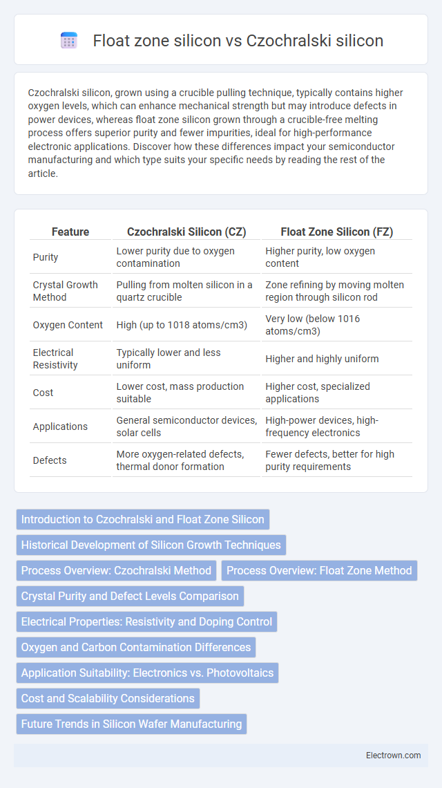
Table of Comparison
| Feature | Czochralski Silicon (CZ) | Float Zone Silicon (FZ) |
|---|---|---|
| Purity | Lower purity due to oxygen contamination | Higher purity, low oxygen content |
| Crystal Growth Method | Pulling from molten silicon in a quartz crucible | Zone refining by moving molten region through silicon rod |
| Oxygen Content | High (up to 1018 atoms/cm3) | Very low (below 1016 atoms/cm3) |
| Electrical Resistivity | Typically lower and less uniform | Higher and highly uniform |
| Cost | Lower cost, mass production suitable | Higher cost, specialized applications |
| Applications | General semiconductor devices, solar cells | High-power devices, high-frequency electronics |
| Defects | More oxygen-related defects, thermal donor formation | Fewer defects, better for high purity requirements |
Introduction to Czochralski and Float Zone Silicon
Czochralski silicon is produced by pulling a single crystal from molten silicon, resulting in large, cylindrical ingots used widely in semiconductor manufacturing due to its affordability and scalability. Float zone silicon, created by melting a narrow region of a silicon rod with a high-frequency induction coil, offers superior purity and fewer defects, making it ideal for high-performance electronic devices. Your choice between these methods depends on the required crystal quality and application, with Czochralski suited for mass production and Float zone for specialized, high-purity needs.
Historical Development of Silicon Growth Techniques
The Czochralski silicon growth technique, developed by Jan Czochralski in 1916, revolutionized semiconductor manufacturing by enabling the production of large, single-crystal silicon boules through the controlled pulling of a seed crystal from molten silicon. Float zone silicon, introduced in the 1950s by William J. Pfann, offers a crucible-free method using localized induction heating to refine high-purity silicon and reduce oxygen contamination compared to Czochralski silicon. Both techniques have evolved to address different industrial demands, with Czochralski silicon dominating large-scale wafer production and Float zone silicon preferred for ultra-high purity applications in power electronics and research.
Process Overview: Czochralski Method
The Czochralski method involves melting high-purity silicon in a crucible and slowly pulling a seed crystal upward while rotating it, allowing a large single crystal ingot to form. This process enables precise control over crystal diameter and doping concentration, making it ideal for producing wafers used in semiconductor manufacturing. Your choice of Czochralski silicon offers scalability and uniformity suitable for integrated circuit fabrication.
Process Overview: Float Zone Method
The Float Zone silicon process involves passing a polycrystalline silicon rod through a radio-frequency induction coil to create a localized molten zone, which moves along the rod to purify the material and form a single crystal. This method avoids contact with a crucible, significantly reducing contamination and resulting in higher purity silicon compared to the Czochralski process. Your choice of silicon for high-performance semiconductor applications may benefit from Float Zone silicon's superior electrical properties and reduced oxygen content.
Crystal Purity and Defect Levels Comparison
Float zone silicon exhibits significantly higher crystal purity compared to Czochralski silicon due to its crucible-free growth process, minimizing contamination from crucible materials. The defect levels in float zone silicon, such as oxygen and carbon impurities, are substantially lower, resulting in superior electrical properties and fewer structural imperfections. Consequently, float zone silicon is preferred for high-performance electronic applications requiring ultra-low impurity concentrations and minimal defect densities.
Electrical Properties: Resistivity and Doping Control
Czochralski silicon typically exhibits lower resistivity levels due to oxygen incorporation during crystal growth, which affects its electrical properties and limits ultra-high purity applications. Float zone silicon offers superior doping control and higher resistivity, reaching values above 10,000 ohm-cm, making it ideal for high-power and high-frequency semiconductor devices. The precise resistivity tuning and reduced oxygen content in float zone silicon ensure enhanced performance in electronic and photovoltaic components compared to Czochralski silicon.
Oxygen and Carbon Contamination Differences
Czochralski silicon typically contains higher oxygen concentrations, ranging from 10^17 to 10^18 atoms/cm3, due to the silicon melt's contact with a quartz crucible, which introduces oxygen contamination. In contrast, Float zone silicon has significantly lower oxygen levels, often below 10^16 atoms/cm3, as the molten zone is suspended without container contact, reducing oxygen pick-up. Carbon contamination is generally low in both methods but can be slightly higher in Float zone silicon due to the use of carbon-containing gases during processing.
Application Suitability: Electronics vs. Photovoltaics
Czochralski silicon, characterized by its lower resistivity and higher impurity levels, is widely favored in electronics manufacturing for integrated circuits and microelectromechanical systems due to its cost-effectiveness and large wafer sizes. Float zone silicon, with its superior purity and high resistivity, is preferred in photovoltaic applications and power devices where high-efficiency solar cells and low defect densities are critical. The selection between these silicon types hinges on balancing electrical performance requirements and economic factors specific to electronics versus photovoltaic industries.
Cost and Scalability Considerations
Czochralski silicon offers lower production costs and higher scalability due to its continuous crystal growth process and widespread industrial adoption, making it suitable for large-volume manufacturing. Float zone silicon, while producing superior purity and fewer defects, incurs higher costs and faces scalability challenges due to its slower, batch-oriented melting process and equipment complexity. The choice between the two techniques depends on balancing cost-efficiency and purity requirements for semiconductor or photovoltaic applications.
Future Trends in Silicon Wafer Manufacturing
Future trends in silicon wafer manufacturing emphasize advancements in both Czochralski (CZ) and Float Zone (FZ) silicon due to their unique advantages. CZ silicon continues to dominate with innovations aimed at reducing oxygen contamination and enhancing crystal uniformity for high-volume semiconductor production. FZ silicon gains traction in power electronics and high-performance applications through ongoing improvements in purity and defect control, driven by increasing demand for efficient energy devices and next-generation integrated circuits.
Czochralski silicon vs Float zone silicon Infographic