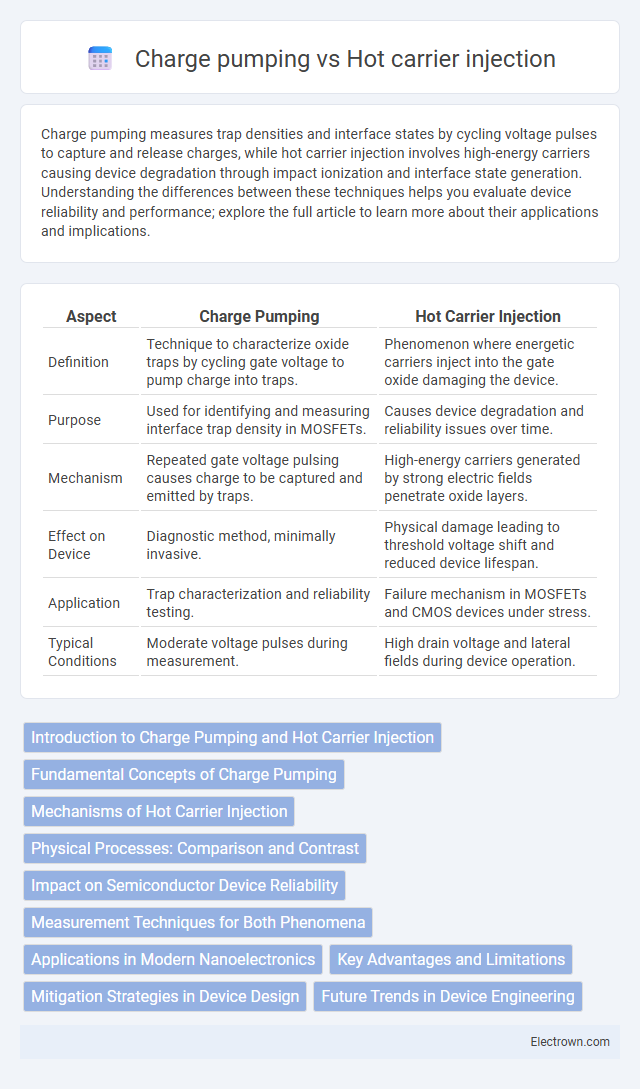
Charge pumping measures trap densities and interface states by cycling voltage pulses to capture and release charges, while hot carrier injection involves high-energy carriers causing device degradation through impact ionization and interface state generation. Understanding the differences between these techniques helps you evaluate device reliability and performance; explore the full article to learn more about their applications and implications.
Table of Comparison
| Aspect | Charge Pumping | Hot Carrier Injection |
|---|---|---|
| Definition | Technique to characterize oxide traps by cycling gate voltage to pump charge into traps. | Phenomenon where energetic carriers inject into the gate oxide damaging the device. |
| Purpose | Used for identifying and measuring interface trap density in MOSFETs. | Causes device degradation and reliability issues over time. |
| Mechanism | Repeated gate voltage pulsing causes charge to be captured and emitted by traps. | High-energy carriers generated by strong electric fields penetrate oxide layers. |
| Effect on Device | Diagnostic method, minimally invasive. | Physical damage leading to threshold voltage shift and reduced device lifespan. |
| Application | Trap characterization and reliability testing. | Failure mechanism in MOSFETs and CMOS devices under stress. |
| Typical Conditions | Moderate voltage pulses during measurement. | High drain voltage and lateral fields during device operation. |
Introduction to Charge Pumping and Hot Carrier Injection
Charge pumping measures interface trap density in MOSFETs by applying a pulsed voltage to the gate, revealing defects that impact device reliability. Hot carrier injection occurs when high-energy carriers damage the semiconductor lattice, causing threshold voltage shifts and degradation over time. Understanding these mechanisms helps you improve transistor performance and longevity in integrated circuits.
Fundamental Concepts of Charge Pumping
Charge pumping is a technique used to characterize interface traps in MOSFETs by applying a pulsed voltage to the gate, causing carriers to be trapped and emitted at defect sites within the silicon oxide interface. This method quantifies interface trap density by measuring the charge displaced during the trap filling and emptying cycles, providing critical insights into device reliability and oxide quality. Unlike hot carrier injection, which involves energetic carriers damaging the oxide and creating traps, charge pumping directly probes existing trap states without inducing additional stress.
Mechanisms of Hot Carrier Injection
Hot carrier injection occurs when high-energy carriers, usually electrons or holes, gain sufficient kinetic energy under high electric fields to overcome potential barriers and become trapped in the gate oxide, leading to device degradation. This process involves carrier acceleration within the semiconductor channel followed by impact ionization or direct injection into the gate dielectric. Compared to charge pumping, which measures interface trap densities via recombination currents, hot carrier injection fundamentally alters device reliability by inducing oxide and interface defects through energetic carrier interactions.
Physical Processes: Comparison and Contrast
Charge pumping involves the trapping and detrapping of charge carriers in the gate oxide traps during switching, leading to interface state generation and threshold voltage shifts. Hot carrier injection occurs when high-energy carriers gain sufficient kinetic energy under strong electric fields to surmount energy barriers and inject into the gate oxide, causing damage to the gate dielectric and interface. Your device's reliability may degrade differently depending on which mechanism predominates, as charge pumping affects trap occupancy cycles while hot carrier injection leads to permanent oxide and interface defects.
Impact on Semiconductor Device Reliability
Charge pumping and hot carrier injection significantly affect semiconductor device reliability by inducing different degradation mechanisms. Charge pumping primarily reveals interface trap states affecting threshold voltage stability and channel conductivity, which can lead to performance drift over time. Hot carrier injection causes energetic carriers to damage the gate oxide and create interface states, accelerating device aging and potentially causing catastrophic failure if not properly managed.
Measurement Techniques for Both Phenomena
Charge pumping measurement involves applying a periodic gate voltage pulse to a MOSFET and monitoring the substrate current to quantify interface trap density, while hot carrier injection is assessed by stressing the device with high electric fields and analyzing changes in threshold voltage and transconductance. Techniques such as DC stress tests, capacitance-voltage (C-V) characterization, and charge pumping are commonly used to study hot carrier effects by tracking degradation over time. Your ability to accurately measure these phenomena influences the reliability evaluation and lifetime prediction of semiconductor devices.
Applications in Modern Nanoelectronics
Charge pumping is a critical technique for evaluating interface trap densities in MOSFETs, essential for improving device reliability and performance in modern nanoelectronics. Hot carrier injection accelerates device aging by introducing traps and defects, impacting the long-term stability of transistors in integrated circuits. Your understanding of these phenomena helps optimize semiconductor device design and ensure enhanced longevity in advanced nanoscale electronic components.
Key Advantages and Limitations
Charge pumping effectively detects and quantifies interface traps in MOSFETs with high sensitivity, enabling precise characterization of device reliability. Hot carrier injection allows controlled stress testing by injecting carriers into the gate oxide, revealing degradation mechanisms but can cause permanent damage if excessive. Your choice between these methods depends on the need for non-destructive testing (favoring charge pumping) versus accelerated lifetime stress analysis (favoring hot carrier injection).
Mitigation Strategies in Device Design
Mitigation strategies for charge pumping emphasize optimizing oxide quality and passivating interface traps to reduce defect generation, while hot carrier injection is controlled by engineering channel doping profiles and using lightly doped drain (LDD) structures to minimize high-energy carrier acceleration. Both phenomena benefit from employing high-k dielectrics and advanced gate stack technologies to enhance reliability and reduce stress-induced degradation. Your device design can further improve robustness by incorporating careful biasing schemes and selecting materials with higher energy barriers to suppress carrier injection effects.
Future Trends in Device Engineering
Future trends in device engineering emphasize minimizing charge pumping and hot carrier injection effects to enhance semiconductor reliability and performance at nanometer scales. Advanced materials like high-k dielectrics and novel transistor architectures such as FinFETs and gate-all-around (GAA) FETs are being developed to reduce interface trap generation and carrier energy buildup. Machine learning algorithms are increasingly applied to predict degradation pathways, enabling more accurate lifetime assessments and optimized device designs.
Charge pumping vs hot carrier injection Infographic