Bulk contact involves direct electrical connection to the semiconductor's bulk region, providing a path for biasing and ensuring device stability, while substrate contact connects to the substrate layer for grounding and minimizing parasitic effects. Understanding the differences between bulk and substrate contacts is essential for optimizing your electronic device performance--read on to explore their unique roles and applications.
Table of Comparison
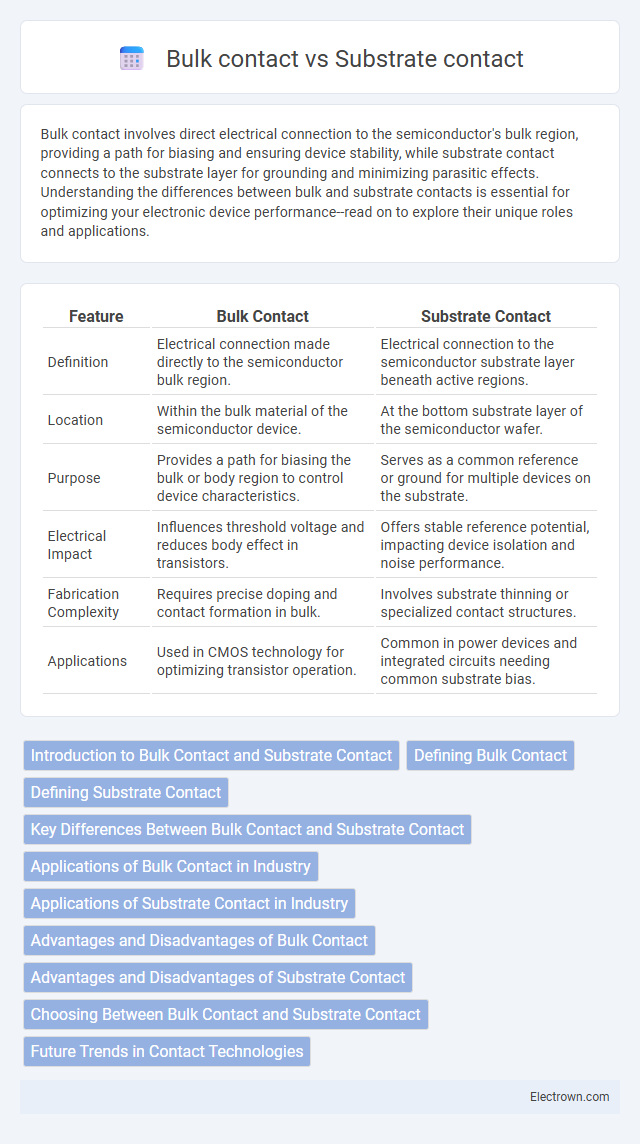
| Feature | Bulk Contact | Substrate Contact |
|---|---|---|
| Definition | Electrical connection made directly to the semiconductor bulk region. | Electrical connection to the semiconductor substrate layer beneath active regions. |
| Location | Within the bulk material of the semiconductor device. | At the bottom substrate layer of the semiconductor wafer. |
| Purpose | Provides a path for biasing the bulk or body region to control device characteristics. | Serves as a common reference or ground for multiple devices on the substrate. |
| Electrical Impact | Influences threshold voltage and reduces body effect in transistors. | Offers stable reference potential, impacting device isolation and noise performance. |
| Fabrication Complexity | Requires precise doping and contact formation in bulk. | Involves substrate thinning or specialized contact structures. |
| Applications | Used in CMOS technology for optimizing transistor operation. | Common in power devices and integrated circuits needing common substrate bias. |
Introduction to Bulk Contact and Substrate Contact
Bulk contact refers to the electrical connection made directly to the bulk semiconductor material in devices like MOSFETs, ensuring proper biasing and minimizing body effect. Substrate contact connects the substrate or body region to a fixed potential, preventing floating body effects and stabilizing transistor operation. Understanding the differences between bulk contact and substrate contact is essential for optimizing your device's electrical performance and reliability.
Defining Bulk Contact
Bulk contact refers to the electrical connection made directly to the substrate or body of a semiconductor device, enabling control of the device's threshold voltage and minimizing parasitic resistances. This type of contact ensures proper voltage biasing and prevents latch-up by stabilizing the potential of the substrate region. Understanding bulk contact is essential for optimizing your device's performance and reliability in integrated circuit applications.
Defining Substrate Contact
Substrate contact refers to the specific electrical connection made directly to the semiconductor substrate in an integrated circuit, enabling effective control of the substrate potential and reducing parasitic effects. Unlike bulk contact, which connects to the bulk material of the wafer, substrate contact ensures proper biasing and isolation within the device's active regions. Understanding substrate contact is crucial for optimizing device performance and minimizing leakage currents in semiconductor designs.
Key Differences Between Bulk Contact and Substrate Contact
Bulk contact refers to the electrical connection made directly to the semiconductor's bulk region, typically within the device's main structure, while substrate contact usually connects to the underlying substrate layer, often serving as a reference potential. Bulk contacts influence the device's bulk potential and can affect leakage currents and latch-up susceptibility, whereas substrate contacts primarily provide a stable reference potential or ground for the device. Understanding these key differences ensures Your semiconductor device achieves optimal performance, reliability, and noise reduction.
Applications of Bulk Contact in Industry
Bulk contact is extensively applied in semiconductor device fabrication, where it ensures reliable electrical connection by providing a low-resistance pathway for current flow within the transistor's bulk material. It is crucial in power electronics and integrated circuits, facilitating efficient current conduction and thermal management in devices such as MOSFETs and BJTs. This contact method improves device performance and reliability in high-power and high-frequency applications across automotive, telecommunications, and consumer electronics industries.
Applications of Substrate Contact in Industry
Substrate contact is widely used in semiconductor device fabrication to provide a stable electrical reference and improve device performance, particularly in MOSFETs and CMOS technologies. This contact method is critical in power electronics, where it ensures efficient heat dissipation and enhanced reliability under high-voltage or high-current conditions. Your designs benefit from substrate contact applications by achieving improved signal integrity and reduced parasitic effects in integrated circuits.
Advantages and Disadvantages of Bulk Contact
Bulk contact offers improved thermal conductivity and reduced electrical resistance compared to substrate contact, enhancing overall device performance and reliability. However, it also introduces challenges such as increased fabrication complexity and potential contamination risks during processing. Understanding these trade-offs helps you optimize semiconductor device designs for specific applications.
Advantages and Disadvantages of Substrate Contact
Substrate contact offers improved electrical isolation and reduced parasitic capacitance compared to bulk contact, enhancing device performance in high-frequency applications. This contact type minimizes latch-up susceptibility and leakage currents, contributing to greater circuit reliability and efficiency. However, substrate contacts can increase fabrication complexity and cost, requiring precise alignment and additional processing steps.
Choosing Between Bulk Contact and Substrate Contact
Choosing between bulk contact and substrate contact hinges on the desired electrical performance and device reliability. Bulk contact offers improved control over the transistor body, reducing latch-up risk and enhancing noise immunity, whereas substrate contact is simpler to implement but may introduce parasitic effects and limited control of the substrate potential. Optimal selection depends on device architecture, process technology, and application-specific electrical requirements.
Future Trends in Contact Technologies
Future trends in contact technologies emphasize the integration of advanced bulk contact designs with novel substrate contact materials to enhance device performance and reliability in semiconductor manufacturing. Innovations include the use of atomically precise substrates and engineered bulk contacts that improve thermal management and electrical conductivity at nanoscale dimensions. Emerging 3D integration techniques and wafer bonding are driving the convergence of bulk and substrate contacts, enabling higher density interconnects and improved signal integrity in next-generation electronic devices.
Bulk contact vs substrate contact Infographic