SiC MOSFETs offer superior performance in high-voltage and high-temperature applications due to their excellent thermal conductivity and high breakdown voltage, while GaN MOSFETs excel in high-frequency and low-loss switching for power electronics. Discover how you can optimize your power system design by exploring the detailed comparison of SiC and GaN MOSFET technologies in the rest of this article.
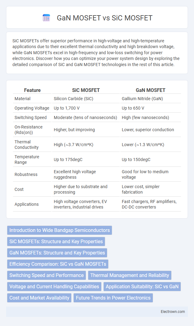
Table of Comparison
| Feature | SiC MOSFET | GaN MOSFET |
|---|---|---|
| Material | Silicon Carbide (SiC) | Gallium Nitride (GaN) |
| Operating Voltage | Up to 1,700 V | Up to 650 V |
| Switching Speed | Moderate (tens of nanoseconds) | High (few nanoseconds) |
| On-Resistance (Rds(on)) | Higher, but improving | Lower, superior conduction |
| Thermal Conductivity | High (~3.7 W/cm*K) | Lower (~1.3 W/cm*K) |
| Temperature Range | Up to 175degC | Up to 150degC |
| Robustness | Excellent high voltage ruggedness | Good for low to medium voltage |
| Cost | Higher due to substrate and processing | Lower cost, simpler fabrication |
| Applications | High voltage converters, EV inverters, industrial drives | Fast chargers, RF amplifiers, DC-DC converters |
Introduction to Wide Bandgap Semiconductors
Wide bandgap semiconductors such as Silicon Carbide (SiC) and Gallium Nitride (GaN) offer superior electrical properties compared to traditional silicon, including higher breakdown voltage, faster switching speeds, and greater thermal conductivity. SiC MOSFETs excel in high-power, high-temperature applications due to their robustness and efficiency, while GaN MOSFETs provide exceptional performance in high-frequency, low-voltage switching scenarios. These materials enable advancements in power electronics, significantly improving energy efficiency and compactness in devices like inverters, chargers, and RF amplifiers.
SiC MOSFETs: Structure and Key Properties
SiC MOSFETs feature a robust silicon carbide semiconductor structure characterized by a wide bandgap of approximately 3.26 eV, enabling high voltage and high-temperature operation. Their key properties include high breakdown electric field strength, superior thermal conductivity around 3.7 W/cm*K, and low on-resistance, which contribute to enhanced efficiency in power switching applications. The layered MOSFET design incorporates a drift region optimized for high blocking voltage, ensuring reliability in demanding environments such as electric vehicles and industrial power supplies.
GaN MOSFETs: Structure and Key Properties
GaN MOSFETs feature a heterostructure with an AlGaN/GaN interface that forms a high electron mobility two-dimensional electron gas (2DEG), enabling high-speed operation and low on-resistance. The wide bandgap of GaN (approximately 3.4 eV) provides excellent thermal stability and high breakdown voltage, making GaN MOSFETs ideal for high-frequency and high-efficiency power conversion applications. These devices offer superior switching performance and reduced gate charge compared to SiC MOSFETs, supporting faster switching speeds and lower conduction losses.
Efficiency Comparison: SiC vs GaN MOSFETs
SiC MOSFETs generally offer higher efficiency in high-voltage applications above 600V due to lower conduction losses and better thermal performance, making them ideal for power conversion in electric vehicles and industrial systems. GaN MOSFETs excel in lower voltage ranges below 600V, providing superior switching speeds and efficiency, which enhances power density and reduces energy loss in fast-switching applications like data centers and consumer electronics. Your choice between SiC and GaN MOSFETs depends largely on the specific voltage and switching frequency requirements to maximize energy efficiency in your system.
Switching Speed and Performance
SiC MOSFETs offer high switching speeds with excellent thermal conductivity, making them ideal for high-power applications requiring robust performance under high voltage and temperature conditions. GaN MOSFETs excel in ultra-fast switching and low on-resistance, providing superior efficiency for high-frequency operations and compact power designs. Your choice depends on the balance between switching speed, efficiency, and thermal management needs in your specific application.
Thermal Management and Reliability
SiC MOSFETs excel in thermal management due to their higher thermal conductivity (~3.7 W/cm*K), enabling better heat dissipation and operation at elevated temperatures up to 175degC compared to GaN MOSFETs, which typically operate below 150degC. The robust material properties of SiC contribute to superior reliability under harsh thermal conditions and prolonged stress cycles, making them ideal for high-power and high-temperature applications. Your choice between SiC and GaN MOSFETs should consider these thermal and reliability parameters based on the specific demands of your power electronics system.
Voltage and Current Handling Capabilities
SiC MOSFETs exhibit superior voltage handling capabilities, typically rated for voltages up to 1700V or higher, making them ideal for high-power, high-voltage applications such as electric vehicles and industrial drives. GaN MOSFETs, while generally limited to lower voltages around 600V to 900V, excel in high-frequency and high-efficiency usage with robust current handling in compact designs. The inherent wide bandgap of SiC enables higher breakdown voltage and thermal conductivity, whereas GaN's fast switching speed offers optimized performance in medium-voltage power conversion systems.
Application Suitability: SiC vs GaN
SiC MOSFETs excel in high-voltage, high-temperature applications such as electric vehicles, industrial motor drives, and renewable energy systems due to their robustness and thermal stability. GaN MOSFETs are ideal for low- to medium-voltage applications like fast chargers, power supplies, and RF amplifiers, offering higher switching speeds and efficiency. Your choice between SiC and GaN should consider voltage requirements, thermal conditions, and switching performance to optimize system reliability and efficiency.
Cost and Market Availability
SiC MOSFETs generally have higher costs due to complex manufacturing processes and limited wafer sizes, while GaN MOSFETs benefit from lower production expenses and increasing economies of scale. Market availability for SiC MOSFETs is well-established in high-power applications, whereas GaN MOSFETs are rapidly expanding in consumer electronics and RF markets. Your choice depends on balancing budget constraints with availability requirements for your specific application.
Future Trends in Power Electronics
SiC MOSFETs offer superior high-voltage performance and thermal conductivity, making them ideal for electric vehicles and grid infrastructure, while GaN MOSFETs excel in high-frequency applications such as wireless charging and fast adapters due to their faster switching speeds. Emerging research focuses on integrating SiC and GaN technologies to optimize efficiency and reduce system size in next-generation power electronics. Your choice between these devices will depend on balancing power handling, switching frequency, and thermal management requirements for future energy-efficient solutions.
SiC MOSFET vs GaN MOSFET Infographic