Thin film electrodes offer higher precision and faster response times due to their uniform thickness and increased surface area, making them ideal for sensitive electrochemical applications. Understanding the differences between thin film and thick film electrodes can enhance your selection process--read on to explore the key advantages and applications of each type.
Table of Comparison
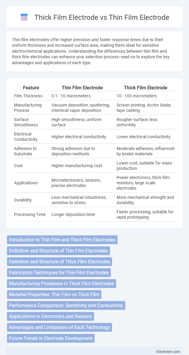
| Feature | Thin Film Electrode | Thick Film Electrode |
|---|---|---|
| Film Thickness | 0.1 - 10 micrometers | 10 - 100 micrometers |
| Manufacturing Process | Vacuum deposition, sputtering, chemical vapor deposition | Screen printing, doctor blade, tape casting |
| Surface Smoothness | High smoothness, uniform surface | Rougher surface, less uniformity |
| Electrical Conductivity | Higher electrical conductivity | Lower electrical conductivity |
| Adhesion to Substrate | Strong adhesion due to deposition methods | Moderate adhesion, influenced by binder materials |
| Cost | Higher manufacturing cost | Lower cost, suitable for mass production |
| Applications | Microelectronics, sensors, precise electrodes | Power electronics, thick film resistors, large scale electrodes |
| Durability | Less mechanical robustness, sensitive to stress | More mechanical strength and durability |
| Processing Time | Longer deposition time | Faster processing, suitable for rapid prototyping |
Introduction to Thin Film and Thick Film Electrodes
Thin film electrodes consist of ultra-thin layers of conductive material deposited on substrates using techniques like sputtering or evaporation, offering high precision and surface uniformity. Thick film electrodes are created by screen-printing conductive pastes composed of metal particles onto ceramic or polymer bases, providing durability and cost-effectiveness for large-scale applications. Your choice between thin film and thick film electrodes depends on the required sensitivity, manufacturing process, and application environment.
Definition and Structure of Thin Film Electrodes
Thin film electrodes consist of ultra-thin layers of conductive materials, typically deposited on substrates using techniques such as sputtering, evaporation, or chemical vapor deposition. Their structure is characterized by minimal thickness, often in the nanometer to micrometer range, enabling high surface area-to-volume ratios and enhanced electrochemical performance. This precise control over thickness and morphology distinguishes thin film electrodes from thick film counterparts, which have significantly greater thickness and porous structures.
Definition and Structure of Thick Film Electrodes
Thick film electrodes are composed of multiple layers of conductive, resistive, or insulating materials deposited as a paste onto a substrate, resulting in a film thickness typically ranging from 10 to 100 micrometers. These layers are often applied through screen printing or similar techniques, followed by a sintering process that solidifies the film and establishes strong adhesion and conductivity. Your choice of thick film electrodes ensures robust mechanical properties and stable electrical performance for applications requiring durability and high current capacity.
Fabrication Techniques for Thin Film Electrodes
Thin film electrodes are fabricated primarily using physical vapor deposition (PVD) and chemical vapor deposition (CVD) techniques, which allow for controlled thickness and uniformity at the nanoscale. These methods enable precise layering and patterning essential for advanced electronic and sensing applications. Your choice of fabrication technique directly influences the electrode's conductivity, adhesion, and overall performance compared to thicker film counterparts.
Manufacturing Processes in Thick Film Electrodes
Thick film electrodes are manufactured using screen printing techniques, where pastes composed of metal or metal oxide particles are deposited onto substrates and subsequently fired at high temperatures to create durable, conductive layers. This process allows for precise control over the film thickness, typically ranging from 10 to 100 micrometers, enabling customization for various sensing or electronic applications. The use of thick film technology offers advantages in scalability, cost-effectiveness, and robustness compared to thin film deposition methods.
Material Properties: Thin Film vs Thick Film
Thin film electrodes exhibit superior uniformity, higher resolution, and enhanced electrical conductivity due to their nanoscale thickness and controlled deposition processes, enabling precise electrochemical performance. Thick film electrodes, composed of multiple micrometer layers, offer increased mechanical durability and higher catalytic activity but may suffer from lower conductivity and reduced surface uniformity. Material composition in thin films is often optimized for specific electronic or sensing applications, while thick films prioritize robustness and cost-effectiveness in large-scale production.
Performance Comparison: Sensitivity and Conductivity
Thin film electrodes exhibit higher sensitivity due to their uniform surface morphology and controlled thickness, enabling enhanced electron transfer rates. Thick film electrodes generally offer greater conductivity because of their bulk material composition but face limitations in sensitivity due to surface roughness and higher resistance paths. The performance trade-off between sensitivity and conductivity depends on the specific application, with thin films excelling in precise sensing and thick films favoring robust electrical conduction.
Applications in Electronics and Sensors
Thin film electrodes offer high precision and miniaturization, making them ideal for microelectronics, biosensors, and flexible wearable devices where surface area and sensitivity are critical. Thick film electrodes provide robustness and cost-effectiveness, commonly used in automotive sensors, industrial gas detection, and large-scale energy storage systems. Both types enable advancements in electronics and sensor technology by balancing performance requirements with manufacturing scalability.
Advantages and Limitations of Each Technology
Thin film electrodes offer superior precision and miniaturization, enabling high-resolution sensing and rapid response times, although they may suffer from higher production costs and limited mechanical durability compared to thick film electrodes. Thick film electrodes provide robust mechanical strength and cost-effective mass production, making them suitable for applications requiring durability, but they often exhibit lower sensitivity and reduced patterning resolution. Selection between thin and thick film technologies depends on application-specific requirements such as sensitivity, cost constraints, and mechanical stress tolerance.
Future Trends in Electrode Development
Future trends in electrode development emphasize enhanced performance and miniaturization for both thin film and thick film electrodes, with thin film electrodes advancing through nanostructured materials to improve sensitivity and flexibility. Thick film electrodes continue evolving with novel paste formulations and printing technologies to increase durability and cost-effectiveness in mass production. You can expect integration of smart sensing capabilities and biocompatible materials to dominate the next generation of electrode innovations.
Thin Film vs Thick Film Electrode Infographic