PCB vias create electrical connections between different layers of a printed circuit board, while blind vias connect outer layers to one or more inner layers without going through the entire board thickness. Understanding these differences can optimize Your PCB design for performance and manufacturing efficiency; continue reading to explore detailed comparisons and applications.
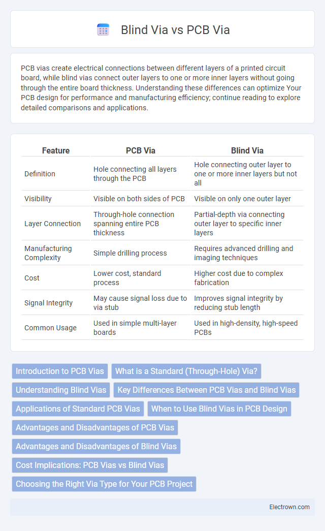
Table of Comparison
| Feature | PCB Via | Blind Via |
|---|---|---|
| Definition | Hole connecting all layers through the PCB | Hole connecting outer layer to one or more inner layers but not all |
| Visibility | Visible on both sides of PCB | Visible on only one outer layer |
| Layer Connection | Through-hole connection spanning entire PCB thickness | Partial-depth via connecting outer layer to specific inner layers |
| Manufacturing Complexity | Simple drilling process | Requires advanced drilling and imaging techniques |
| Cost | Lower cost, standard process | Higher cost due to complex fabrication |
| Signal Integrity | May cause signal loss due to via stub | Improves signal integrity by reducing stub length |
| Common Usage | Used in simple multi-layer boards | Used in high-density, high-speed PCBs |
Introduction to PCB Vias
PCB vias are essential conductive pathways that connect different layers within a printed circuit board, enabling efficient electrical signals transmission. Standard through-hole vias pass entirely through the board, while blind vias connect outer layers to one or more inner layers without penetrating the entire board thickness. Understanding the differences between via types helps optimize your PCB design for space, signal integrity, and manufacturing complexity.
What is a Standard (Through-Hole) Via?
A standard (through-hole) via is a plated hole that electrically connects all layers of a multi-layer printed circuit board (PCB) by passing through its entire thickness. This via type enables signal and power transmission across inner and outer layers, providing robust mechanical support during assembly. Through-hole vias are widely used due to their simplicity and cost-effectiveness in PCB manufacturing, despite occupying more space compared to blind vias.
Understanding Blind Vias
Blind vias are used in printed circuit boards (PCBs) to connect outer layers to one or more inner layers without penetrating the entire board, enhancing signal integrity and reducing electromagnetic interference. Unlike through-hole vias, blind vias save space and improve routing density by only extending partially through the PCB stack-up. Understanding their role in multilayer designs is crucial for optimizing electrical performance and manufacturing efficiency in advanced electronics.
Key Differences Between PCB Vias and Blind Vias
PCB vias are through-hole connections that pass entirely through the board, enabling signal or power transfer between all layers, while blind vias connect an outer layer to one or more inner layers without penetrating the entire board. Blind vias improve board density and performance by minimizing space usage and reducing signal interference, making them ideal for complex, multi-layer PCB designs. Understanding the key differences helps optimize your PCB layout for manufacturing cost, electrical performance, and design complexity.
Applications of Standard PCB Vias
Standard PCB vias serve as essential electrical connections between different layers in multilayer printed circuit boards, facilitating signal and power transmission. They are commonly used in applications requiring straightforward interlayer connectivity, such as in consumer electronics, automotive control units, and industrial machinery. Your circuit designs benefit from the cost-effectiveness and reliability of these through-hole vias in both prototyping and mass production environments.
When to Use Blind Vias in PCB Design
Blind vias are ideal in PCB design when routing space is limited and connections are needed between outer layers and one or more inner layers without passing through the entire board. You should use blind vias to improve signal integrity and reduce board size in high-density, multi-layer PCBs where through-hole vias may cause signal interference or take up excessive space. Choosing blind vias enhances electrical performance and allows for more compact, reliable circuit layouts.
Advantages and Disadvantages of PCB Vias
PCB vias serve as electrical connections between different layers of a printed circuit board, with through-hole vias passing completely through the board and blind vias connecting outer layers to inner layers without penetrating the entire board. Through-hole vias offer greater mechanical strength and easier inspection but consume more space and can cause signal integrity issues due to increased parasitic inductance. Blind vias save board space and improve signal performance in high-density designs but are more complex and expensive to manufacture, with limited thermal relief and reduced reliability in some cases.
Advantages and Disadvantages of Blind Vias
Blind vias in PCB design provide the advantage of saving board space by connecting outer layers to one or more inner layers without passing through the entire board, enhancing signal integrity and allowing higher component density. However, blind vias require advanced manufacturing processes, increasing production costs and complexity, and can complicate inspection and repair due to limited accessibility. Despite these challenges, their use is crucial in high-density interconnect (HDI) boards where minimizing space and maintaining performance are priorities.
Cost Implications: PCB Vias vs Blind Vias
PCB vias typically incur lower manufacturing costs due to their simpler through-hole drilling process and standard production techniques. Blind vias require advanced fabrication methods like laser drilling or sequential lamination, significantly increasing production expenses and complexity. Cost considerations often lead designers to use PCB vias for less critical layers and reserve blind vias for high-density interconnects where space-saving justifies the premium.
Choosing the Right Via Type for Your PCB Project
Selecting the appropriate via type for your PCB project depends on factors like layer count, electrical performance, and manufacturing cost. Blind vias connect outer layers to one or more inner layers without passing through the entire board, ideal for high-density designs requiring space optimization. Through-hole vias pass through all layers, offering robust electrical and mechanical connections but occupying more space and possibly increasing signal interference.
PCB Via vs Blind Via Infographic