Schematic diagrams represent the electrical connections and components in a circuit using symbols, serving as a blueprint for understanding the design, while PCBs (Printed Circuit Boards) provide the physical platform where those schematics are realized by mounting and interconnecting components. Understanding the differences between schematics and PCBs will enhance Your ability to navigate electronic design and assembly processes; read on to explore these concepts in detail.
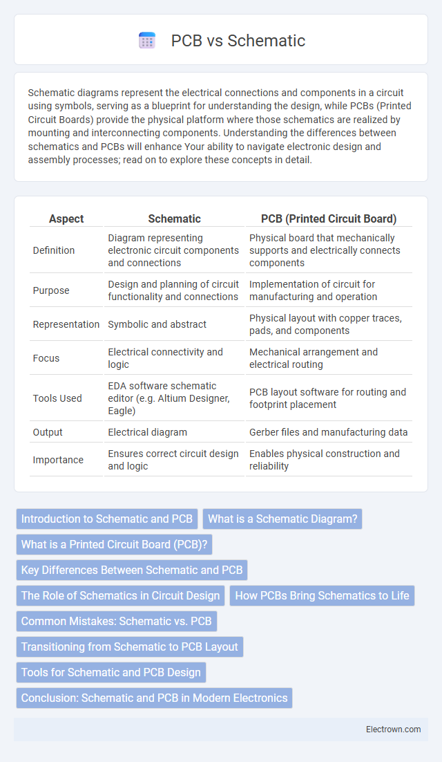
Table of Comparison
| Aspect | Schematic | PCB (Printed Circuit Board) |
|---|---|---|
| Definition | Diagram representing electronic circuit components and connections | Physical board that mechanically supports and electrically connects components |
| Purpose | Design and planning of circuit functionality and connections | Implementation of circuit for manufacturing and operation |
| Representation | Symbolic and abstract | Physical layout with copper traces, pads, and components |
| Focus | Electrical connectivity and logic | Mechanical arrangement and electrical routing |
| Tools Used | EDA software schematic editor (e.g. Altium Designer, Eagle) | PCB layout software for routing and footprint placement |
| Output | Electrical diagram | Gerber files and manufacturing data |
| Importance | Ensures correct circuit design and logic | Enables physical construction and reliability |
Introduction to Schematic and PCB
A schematic diagram represents the electrical connections and components in a circuit using standardized symbols, serving as a blueprint for designing and understanding the circuit's functionality. A Printed Circuit Board (PCB) translates this schematic into a physical layout, where components are mounted and connected through conductive pathways on a non-conductive substrate. You rely on the schematic to accurately design the PCB, ensuring your electronic device functions correctly.
What is a Schematic Diagram?
A schematic diagram is a detailed representation of an electronic circuit using standardized symbols to illustrate components and their connections, serving as the blueprint for designing a PCB (Printed Circuit Board). It focuses on the logical flow and relationships between components rather than the physical layout, allowing engineers to visualize circuit functionality clearly. Your ability to interpret schematic diagrams is essential for troubleshooting, modifying, or designing efficient and error-free electronic circuits before PCB fabrication.
What is a Printed Circuit Board (PCB)?
A Printed Circuit Board (PCB) is a flat, insulating board used to mechanically support and electrically connect electronic components through conductive pathways etched from copper sheets. PCBs replace traditional wiring systems by providing a compact, reliable platform for assembling circuits, enabling efficient signal transmission and power distribution. They are essential in modern electronics, ranging from simple gadgets to complex devices like computers and smartphones.
Key Differences Between Schematic and PCB
A schematic represents the electrical connections and components in a circuit using symbols, focusing on the functional aspects and signal flow. A PCB (Printed Circuit Board) translates that schematic into a physical layout, showing the exact placement of components and copper traces for manufacturing. Your ability to design efficient electronics depends on understanding how schematics guide the logical design while PCBs enable the practical hardware implementation.
The Role of Schematics in Circuit Design
Schematics serve as the foundational blueprint in circuit design, illustrating the logical connections and components before physical implementation on a PCB. These diagrams help engineers visualize the electrical relationships, identify potential issues, and plan component placement effectively. Understanding the schematic's role ensures Your design process is efficient, reducing errors during PCB layout and manufacturing.
How PCBs Bring Schematics to Life
Printed Circuit Boards (PCBs) transform schematic diagrams into tangible electronic devices by physically connecting components according to the circuit design. While schematics represent the electrical connections symbolically, PCBs organize and mount components on a conductive substrate, ensuring accurate signal paths and mechanical stability. Your ability to prototype and manufacture complex electronics relies heavily on the precision with which PCBs translate schematic blueprints into functional hardware.
Common Mistakes: Schematic vs. PCB
Common mistakes in schematic vs. PCB design often stem from mismatched component footprints and incorrect net connections, leading to errors in physical layout and functionality. Overlooking the translation of schematic symbols to accurate PCB footprints causes misaligned placements and routing issues that compromise signal integrity. Ensuring strict cross-verification between schematic diagrams and PCB layouts reduces errors and improves overall circuit reliability.
Transitioning from Schematic to PCB Layout
Transitioning from schematic to PCB layout involves converting the circuit design into a physical board representation, ensuring all electrical connections are accurately mapped to appropriate pads and traces. Specialized software tools facilitate this process by importing netlists from schematics, enabling component placement and routing to optimize signal integrity and manufacturability. Design rule checks (DRC) and simulation are critical steps to verify that the PCB layout meets electrical and mechanical specifications before fabrication.
Tools for Schematic and PCB Design
Schematic design tools like Altium Designer, Eagle, and KiCad allow you to create detailed circuit diagrams by placing and connecting electronic components symbolically. PCB design software, such as Mentor Graphics PADS, OrCAD PCB Designer, and DipTrace, enables precise layout of physical board layers, routing paths, and component footprints. Your workflow benefits from seamless integration between schematic capture and PCB layout tools, ensuring accurate translation of circuit designs into manufacturable printed circuit boards.
Conclusion: Schematic and PCB in Modern Electronics
Schematic diagrams serve as the blueprint for electronic circuits, detailing component connections and functions, while PCBs provide the physical platform for assembling these components with precise wiring and layout. Efficient electronics design relies on seamless integration of schematics and PCBs, ensuring accuracy, signal integrity, and manufacturability. Mastery of both schematic creation and PCB layout is essential for optimizing performance and reducing errors in modern electronic devices.
Schematic vs PCB Infographic