Latch-up occurs when a parasitic structure within an integrated circuit creates a low-impedance path, causing high current flow and potential device failure, while cross-talk refers to unwanted interference between signal lines due to electromagnetic coupling. Understanding these effects is crucial to improving your circuit's reliability and performance; explore the rest of the article to learn how to mitigate latch-up and cross-talk in your designs.
Table of Comparison
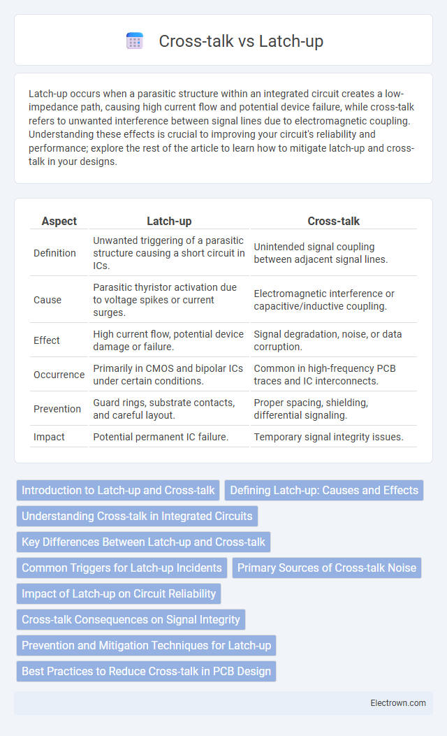
| Aspect | Latch-up | Cross-talk |
|---|---|---|
| Definition | Unwanted triggering of a parasitic structure causing a short circuit in ICs. | Unintended signal coupling between adjacent signal lines. |
| Cause | Parasitic thyristor activation due to voltage spikes or current surges. | Electromagnetic interference or capacitive/inductive coupling. |
| Effect | High current flow, potential device damage or failure. | Signal degradation, noise, or data corruption. |
| Occurrence | Primarily in CMOS and bipolar ICs under certain conditions. | Common in high-frequency PCB traces and IC interconnects. |
| Prevention | Guard rings, substrate contacts, and careful layout. | Proper spacing, shielding, differential signaling. |
| Impact | Potential permanent IC failure. | Temporary signal integrity issues. |
Introduction to Latch-up and Cross-talk
Latch-up is a short circuit condition in CMOS integrated circuits caused by the unintended activation of parasitic thyristors, leading to device malfunction or destruction. Cross-talk refers to the unwanted interference caused by capacitive, inductive, or conductive coupling between adjacent signal lines in electronic circuits, degrading signal integrity. Both phenomena pose significant challenges to the reliability and performance of microelectronic devices.
Defining Latch-up: Causes and Effects
Latch-up is a failure mechanism in CMOS devices caused by the unintended activation of parasitic thyristor structures, triggered by voltage spikes or ionizing radiation. This phenomenon leads to high current flow, potentially damaging the integrated circuit by causing thermal runaway or permanent latch-up state. Understanding latch-up origins helps you mitigate risks in semiconductor design, differentiating it from cross-talk, which involves unwanted signal interference rather than destructive current flow.
Understanding Cross-talk in Integrated Circuits
Cross-talk in integrated circuits occurs when unwanted electromagnetic interference from adjacent signal lines induces noise, causing potential data corruption or signal integrity issues. This phenomenon often results from capacitive or inductive coupling in tightly packed IC layouts, especially at high frequencies. Understanding cross-talk helps you implement design strategies such as shielding, spacing, and proper routing to minimize its impact on circuit performance.
Key Differences Between Latch-up and Cross-talk
Latch-up occurs when unintended parasitic structures in integrated circuits create a low-impedance path, causing high current flow and potential device failure, while cross-talk refers to unwanted signal interference between adjacent conductive lines due to capacitive or inductive coupling. Latch-up primarily affects the stability and reliability of the device by triggering short circuits, whereas cross-talk degrades signal integrity, leading to data errors and noise. Understanding these key differences helps you design circuits with improved protection mechanisms and enhanced performance.
Common Triggers for Latch-up Incidents
Common triggers for latch-up incidents include transient voltage spikes, high current flow resulting from ionizing radiation, and improper biasing in CMOS circuits. Electrostatic discharge (ESD) and power supply fluctuations also frequently initiate parasitic thyristor activation leading to latch-up. Understanding these triggers is critical for designing robust integrated circuits to prevent device failure.
Primary Sources of Cross-talk Noise
Cross-talk noise primarily originates from capacitive coupling, inductive coupling, and substrate coupling between adjacent signal lines in integrated circuits. Capacitive coupling occurs due to the electric field interaction between closely spaced conductors, while inductive coupling results from magnetic fields generated by changing currents in neighboring lines. Substrate coupling happens when signals interfere through the semiconductor substrate, leading to unintended noise in sensitive circuit nodes.
Impact of Latch-up on Circuit Reliability
Latch-up causes significant reliability issues in integrated circuits by creating low-impedance paths that lead to excessive current flow, potentially damaging the device permanently. This phenomenon disrupts normal circuit operation and accelerates degradation, reducing the overall lifespan of semiconductor components. Effective mitigation techniques, such as guard rings and substrate biasing, are crucial to maintain circuit stability and prevent catastrophic failures.
Cross-talk Consequences on Signal Integrity
Cross-talk induces unwanted coupling between adjacent signal lines, leading to noise interference and signal distortion that significantly degrade signal integrity. The capacitive and inductive coupling effects cause timing errors, increased bit error rates, and potential data corruption in high-speed digital circuits. Mitigating cross-talk through improved layout techniques and shielding is essential to maintain reliable signal transmission and optimize overall system performance.
Prevention and Mitigation Techniques for Latch-up
Latch-up prevention and mitigation techniques primarily involve careful design practices such as incorporating guard rings and well taps to isolate parasitic thyristors in CMOS circuits. Using substrates with higher resistivity and optimizing layout spacing reduces the risk of latch-up by minimizing current injection paths. You can also enhance reliability by controlling power supply voltage ramps and incorporating current limiting circuits to prevent excessive transient currents that trigger latch-up.
Best Practices to Reduce Cross-talk in PCB Design
Minimizing cross-talk in PCB design involves increasing the spacing between signal traces and using ground or power planes as shields to reduce electromagnetic interference. Employing differential signaling and controlled impedance routing also helps maintain signal integrity by mitigating unwanted coupling. You can enhance performance by carefully planning trace layouts and implementing proper decoupling techniques to effectively reduce cross-talk.
Latch-up vs cross-talk Infographic