Schematic capture involves creating a detailed electrical diagram that defines component connections, while PCB layout focuses on arranging those components physically on the board for manufacturing. Explore the differences further to understand how each step impacts Your design process.
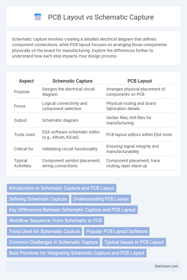
Table of Comparison
| Aspect | Schematic Capture | PCB Layout |
|---|---|---|
| Purpose | Designs the electrical circuit diagram | Arranges physical placement of components on PCB |
| Focus | Logical connectivity and component selection | Physical routing and board fabrication details |
| Output | Schematic diagram | Gerber files, drill files for manufacturing |
| Tools Used | EDA software schematic editor (e.g., Altium, KiCad) | PCB layout editors within EDA tools |
| Critical for | Validating circuit functionality | Ensuring signal integrity and manufacturability |
| Typical Activities | Component symbol placement, wiring connections | Component placement, trace routing, layer stack-up |
Introduction to Schematic Capture and PCB Layout
Schematic capture is the process of creating an electrical diagram that represents the components and connections of a circuit, serving as the blueprint for electronic design. PCB layout involves transforming the schematic into a physical design that places components and routes electrical traces on a printed circuit board. Your ability to efficiently move from schematic capture to PCB layout is crucial for accurate circuit manufacturing and functional reliability.
Defining Schematic Capture
Schematic capture involves the precise creation of an electrical diagram that represents the circuit's components and their interconnections using standardized symbols. This foundational step lays out the logical design and connectivity, serving as the blueprint for subsequent PCB layout. Your accuracy during schematic capture directly impacts the efficiency and functionality of the final printed circuit board design.
Understanding PCB Layout
PCB layout involves translating the schematic capture into a physical design, focusing on component placement, routing of electrical connections, and ensuring signal integrity. Understanding PCB layout requires knowledge of design rules, layer stack-up, and thermal management to optimize performance and manufacturability. Your ability to effectively manage these factors ensures the final product meets both functional and production requirements.
Key Differences Between Schematic Capture and PCB Layout
Schematic capture involves creating a detailed electronic diagram that defines the electrical connections and components of a circuit, serving as the blueprint for the design. PCB layout translates this schematic into a physical board design, focusing on component placement, routing pathways, and ensuring electrical and mechanical constraints are met. Key differences include schematic capture prioritizing logical connectivity and functionality, while PCB layout emphasizes physical arrangement and signal integrity for manufacturability.
Workflow Sequence: From Schematic to PCB
The workflow sequence from schematic capture to PCB layout begins with creating an accurate schematic diagram that defines the electrical connections and components in the circuit. Once the schematic is complete, design data is transferred to the PCB layout software, where component placement and routing of electrical connections on the printed circuit board are performed. Your efficient transition through these stages ensures a seamless design process, reducing errors and optimizing board functionality.
Tools Used for Schematic Capture
Schematic capture relies on specialized software tools such as Altium Designer, Eagle, OrCAD Capture, and KiCad, enabling engineers to create precise electronic circuit diagrams. These tools offer libraries of standardized components, enabling efficient symbol placement and connection verification. The accuracy and clarity provided by schematic capture tools are essential for seamless transition to PCB layout and manufacturing processes.
Popular PCB Layout Software
Popular PCB layout software like Altium Designer, Eagle, and KiCad integrate both schematic capture and PCB layout functionalities, enabling engineers to transition seamlessly from circuit design to physical board layout. These tools feature advanced routing algorithms, real-time design rule checks, and extensive component libraries, facilitating efficient and error-free PCB design. By supporting collaborative workflows and 3D visualization, they enhance design accuracy and accelerate prototype development.
Common Challenges in Schematic Capture
Schematic capture often faces challenges such as managing complex circuit designs, ensuring accurate component symbols, and maintaining proper connectivity to prevent errors during PCB layout. Errors in wiring or component placement during schematic capture can lead to significant issues in the final PCB manufacturing process. You must carefully validate your schematic to avoid costly revisions and ensure a smooth transition to the PCB layout stage.
Typical Issues in PCB Layout
Typical issues in PCB layout include signal integrity problems such as crosstalk, electromagnetic interference (EMI), and improper trace impedance leading to data errors and noise. Poor component placement and inadequate power distribution can cause thermal hotspots and voltage drops, affecting overall circuit performance. Additionally, routing constraints like insufficient clearance, inefficient layer stack-up, and incorrect pad sizes often result in manufacturability challenges and increased production costs.
Best Practices for Integrating Schematic Capture and PCB Layout
Integrating schematic capture and PCB layout efficiently requires maintaining a clear and organized design hierarchy, ensuring consistent net naming conventions between the schematic and layout files. Utilize design rule checks (DRCs) early and often to catch connectivity errors and component placement issues before proceeding to fabrication. Your workflow should incorporate bi-directional synchronization tools that enable seamless updates between the schematic and PCB layout, reducing errors and saving time in the design process.
Schematic capture vs PCB layout Infographic