Junction capacitance refers to the capacitance formed at the PN junction in semiconductor devices, directly affecting device speed and leakage current, while overlap capacitance arises from the physical overlap between the gate electrode and the source/drain regions, influencing parasitic capacitance and switching behavior. Understanding these capacitances is crucial for optimizing your circuit's performance and power efficiency; explore the full article to learn how each impacts device operation and design choices.
Table of Comparison
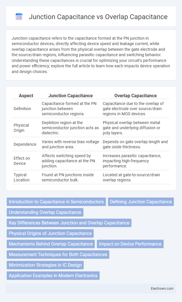
| Aspect | Junction Capacitance | Overlap Capacitance |
|---|---|---|
| Definition | Capacitance formed at the PN junction between semiconductor regions. | Capacitance due to the overlap of gate electrode over source/drain regions in MOS devices. |
| Physical Origin | Depletion region at the semiconductor junction acts as dielectric. | Physical overlap between metal gate and underlying diffusion or poly layers. |
| Dependence | Varies with reverse bias voltage and junction area. | Depends on gate overlap length and gate oxide thickness. |
| Effect on Device | Affects switching speed by adding capacitance at the PN junction. | Increases parasitic capacitance, impacting high-frequency performance. |
| Typical Location | Found at PN junctions inside semiconductor bulk. | Located at gate-to-source/drain overlap regions. |
Introduction to Capacitance in Semiconductors
Capacitance in semiconductors arises from the ability of p-n junctions and overlapping metal layers to store charge, fundamentally influencing device performance. Junction capacitance occurs at the depletion region of a p-n junction, varying with applied voltage and impacting switching speed. Overlap capacitance, caused by the electric field between overlapping gate and source/drain regions, affects high-frequency device operation and your circuit's frequency response.
Defining Junction Capacitance
Junction capacitance, also known as depletion capacitance, arises at the p-n junction of a semiconductor device due to the depletion region acting as a dielectric between charged regions. It varies with the applied voltage, influencing the overall capacitance and switching speed of devices like diodes and MOSFETs. Understanding junction capacitance is crucial for optimizing Your circuit's high-frequency performance and minimizing signal distortion.
Understanding Overlap Capacitance
Overlap capacitance occurs where the gate electrode overlaps the source or drain regions, creating a capacitive effect due to the electric field interaction between these areas. This capacitance significantly influences the switching speed and power consumption in MOSFET devices by adding to the total gate capacitance. Unlike junction capacitance, which arises from the depletion region between semiconductor junctions, overlap capacitance is determined by device geometry and gate-to-source/drain overlap length.
Key Differences Between Junction and Overlap Capacitance
Junction capacitance arises from the depletion region between semiconductor junctions, directly influenced by doping concentration and applied voltage, making it voltage-dependent. Overlap capacitance occurs due to the lateral overlap of gate and source/drain regions, primarily determined by the physical gate-to-channel overlap and oxide thickness, remaining relatively constant with voltage changes. Your circuit's performance in high-frequency applications can be optimized by minimizing overlap capacitance to reduce parasitic effects, while managing junction capacitance to control transient response and switching speed.
Physical Origins of Junction Capacitance
Junction capacitance arises from the depletion region formed between p-n junctions in semiconductor devices, where the separation of charges creates a voltage-dependent capacitor effect. This capacitance is fundamentally linked to the width of the depletion layer, which varies with the applied reverse-bias voltage, altering the charge storage capacity. Unlike overlap capacitance, which results from the physical overlap of gate and source/drain electrodes, junction capacitance is intrinsic to the semiconductor junction's electrostatic properties.
Mechanisms Behind Overlap Capacitance
Overlap capacitance arises from the electric field coupling between the gate electrode and the source/drain regions in a MOSFET, where the gate extends slightly over the source and drain diffusion areas. This capacitance is influenced by the gate oxide thickness, the gate length, and the lateral overlap distance, creating a parasitic effect that adds to the total input capacitance. Unlike junction capacitance, which is formed at the p-n junctions between the source/drain and the substrate, overlap capacitance is primarily governed by the physical gate-to-diffusion overlap and the inherent dielectric properties of the gate oxide layer.
Impact on Device Performance
Junction capacitance affects the switching speed and frequency response by introducing charge storage at the pn-junction, which can slow down device operation in high-speed circuits. Overlap capacitance, caused by the overlap of gate and source/drain regions, impacts the input capacitance and contributes to increased power consumption and noise in MOSFET devices. Optimizing your device design to minimize both capacitances is crucial for enhancing overall performance, especially in RF and high-frequency applications.
Measurement Techniques for Both Capacitances
Measurement techniques for junction capacitance typically involve capacitance-voltage (C-V) profiling using precision LCR meters or impedance analyzers to characterize the depletion region's voltage-dependent behavior. Overlap capacitance measurement requires high-frequency S-parameter analysis and de-embedding methods to isolate parasitic capacitances caused by lithographic overlaps in MOSFET gate structures. Both capacitances are often extracted through specialized test structures and device simulation models to ensure accuracy in advanced semiconductor process characterization.
Minimization Strategies in IC Design
Minimizing junction capacitance in IC design involves reducing depletion region areas through careful doping profile optimization and using guard rings to isolate devices. Overlap capacitance can be lowered by precise gate-to-source/drain alignment and employing thinner gate oxides with high-k dielectric materials to reduce parasitic overlap effects. Your design choices in transistor layout and material selection directly impact the balance between junction and overlap capacitance, crucial for improving overall circuit speed and power efficiency.
Application Examples in Modern Electronics
Junction capacitance is crucial in designing high-speed semiconductor devices such as diodes and transistors, where controlling the depletion region affects switching speeds and power efficiency. Overlap capacitance plays a significant role in MOSFETs and integrated circuits, impacting gate delay and signal integrity by influencing the overlap between the gate electrode and source/drain regions. Understanding the differences helps optimize your circuit performance in RF amplifiers, high-frequency oscillators, and advanced microprocessors.
Junction Capacitance vs Overlap Capacitance Infographic