Floating gate memory stores charge on a conductive floating gate to maintain data retention, while charge trap memory uses an insulating layer to trap charges, offering improved scalability and reliability. Explore the rest of the article to understand how these differences impact your choice in non-volatile memory technologies.
Table of Comparison
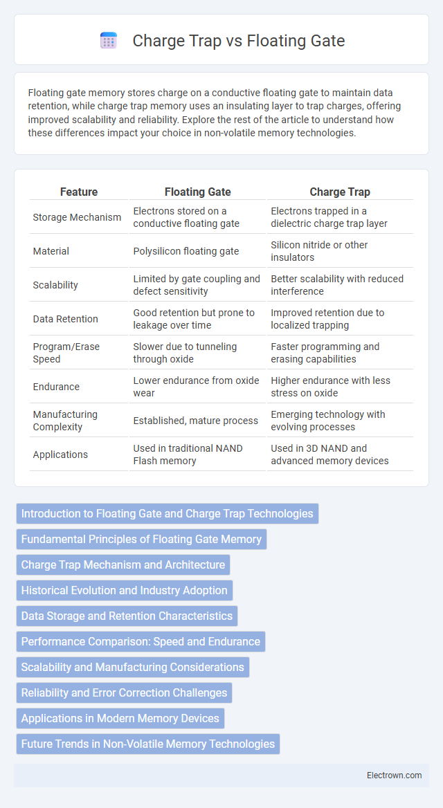
| Feature | Floating Gate | Charge Trap |
|---|---|---|
| Storage Mechanism | Electrons stored on a conductive floating gate | Electrons trapped in a dielectric charge trap layer |
| Material | Polysilicon floating gate | Silicon nitride or other insulators |
| Scalability | Limited by gate coupling and defect sensitivity | Better scalability with reduced interference |
| Data Retention | Good retention but prone to leakage over time | Improved retention due to localized trapping |
| Program/Erase Speed | Slower due to tunneling through oxide | Faster programming and erasing capabilities |
| Endurance | Lower endurance from oxide wear | Higher endurance with less stress on oxide |
| Manufacturing Complexity | Established, mature process | Emerging technology with evolving processes |
| Applications | Used in traditional NAND Flash memory | Used in 3D NAND and advanced memory devices |
Introduction to Floating Gate and Charge Trap Technologies
Floating Gate technology uses a conductive floating gate insulated by oxide layers to store electrical charges, enabling non-volatile memory retention in devices like NAND flash. Charge Trap technology stores charges in a dielectric layer or traps within an insulating material rather than a conductive gate, enhancing scalability and reducing interference in advanced memory structures. Both technologies are pivotal in modern semiconductor memory, with Floating Gate excelling in proven reliability and Charge Trap offering improved endurance and size reduction for high-density applications.
Fundamental Principles of Floating Gate Memory
Floating gate memory stores charge on a conductive floating gate insulated by a thin oxide layer, enabling non-volatile data retention through electron tunneling. The fundamental principle relies on the trapped charge modulating the threshold voltage of the transistor, representing binary data. This charge storage mechanism ensures high endurance and stable retention in flash memory cells.
Charge Trap Mechanism and Architecture
Charge Trap memory utilizes an insulating layer, typically silicon nitride, to store charge within localized traps, enabling precise charge retention and reducing leakage compared to Floating Gate cells that store charge in a conductive polysilicon gate. The Charge Trap architecture separates the storage layer from the channel with tunneling oxide, enhancing scalability and endurance by minimizing charge loss and oxide wear. This mechanism allows for smaller cell size and improved reliability in advanced non-volatile memory technologies such as 3D NAND and NOR Flash.
Historical Evolution and Industry Adoption
Floating gate technology, first introduced in the 1960s, revolutionized non-volatile memory with its use in EEPROM and NAND flash, establishing itself as the industry standard for decades due to its reliable charge storage capability within a conductive floating gate. Charge trap memory emerged later, utilizing silicon nitride layers to store charge, offering advantages in scaling, endurance, and simpler manufacturing, which has led to increased adoption in advanced nodes by major semiconductor companies like Toshiba and Samsung. Your choice between these technologies should consider the evolutionary maturity of floating gate devices versus the scaling benefits and industry trend favoring charge trap in modern, high-density memory applications.
Data Storage and Retention Characteristics
Floating Gate memory stores data by trapping electrons on a conductive polysilicon layer, offering strong data retention with a typical lifespan of over 10 years due to its stable charge storage. Charge Trap memory uses insulating materials like silicon nitride to capture charges, enabling faster programming speeds and better scalability but generally exhibiting shorter retention times compared to floating gate cells. Your choice depends on whether long-term data stability or scaling and performance are prioritized in the application.
Performance Comparison: Speed and Endurance
Floating gate memory typically offers faster write and erase speeds due to its well-established tunnel oxide mechanisms, making it ideal for high-performance applications. Charge trap memory, however, excels in endurance with better tolerance to high voltage stress and less electron leakage, extending the device's lifespan under repeated program/erase cycles. You should consider floating gate for speed-critical tasks and charge trap when long-term reliability and endurance are paramount.
Scalability and Manufacturing Considerations
Floating Gate technology faces scalability challenges as shrinking device dimensions increase interference and charge leakage risks, complicating manufacturing precision. Charge Trap memory offers better scalability due to its simpler structure and reduced interference, enabling continued miniaturization with fewer defects. Your choice of memory technology will significantly impact manufacturing yield and integration with advanced semiconductor processes.
Reliability and Error Correction Challenges
Floating Gate memory cells face significant challenges in reliability due to charge leakage and cell-to-cell interference, which can lead to data retention issues and increased error rates. Charge Trap technology offers improved endurance and retention by using localized charge storage in an insulating layer, but it requires sophisticated error correction algorithms to mitigate disturbances like program/erase cycling-induced charge trapping variability. Both memory types necessitate advanced error correction techniques, such as ECC and adaptive read thresholds, to enhance overall data integrity and device lifespan in modern NAND flash applications.
Applications in Modern Memory Devices
Floating gate technology is widely used in traditional NAND flash memory, offering reliable data retention and cost-effective storage solutions for USB drives, SSDs, and memory cards. Charge trap memory, found in modern 3D NAND devices, enhances scalability and endurance by storing charges in silicon nitride layers, improving performance in high-density storage applications. Your choice between floating gate and charge trap can impact device lifespan, data retention, and overall efficiency in consumer electronics and enterprise storage systems.
Future Trends in Non-Volatile Memory Technologies
Floating Gate and Charge Trap technologies will play critical roles in the future landscape of non-volatile memory (NVM), with Charge Trap memory gaining momentum due to its scalability and lower power consumption compared to traditional Floating Gate designs. Emerging trends focus on integrating Charge Trap NVM in 3D architectures, enhancing density and endurance for advanced applications such as AI and IoT devices. Your choice of memory technology will increasingly depend on factors like reliability, endurance, and the ability to support high-speed data retention in evolving semiconductor manufacturing processes.
Floating Gate vs Charge Trap Infographic