PMOS pullup transistors are commonly used in CMOS technology for their ability to efficiently connect the output to the positive supply voltage with low resistance, resulting in better power efficiency during the high output state. Understanding the differences between PMOS pullup and NMOS pullup is crucial for optimizing your circuit's performance, so explore the rest of this article to learn more.
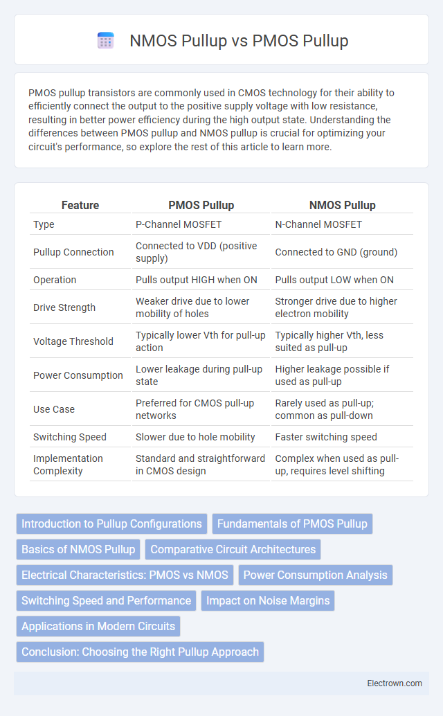
Table of Comparison
| Feature | PMOS Pullup | NMOS Pullup |
|---|---|---|
| Type | P-Channel MOSFET | N-Channel MOSFET |
| Pullup Connection | Connected to VDD (positive supply) | Connected to GND (ground) |
| Operation | Pulls output HIGH when ON | Pulls output LOW when ON |
| Drive Strength | Weaker drive due to lower mobility of holes | Stronger drive due to higher electron mobility |
| Voltage Threshold | Typically lower Vth for pull-up action | Typically higher Vth, less suited as pull-up |
| Power Consumption | Lower leakage during pull-up state | Higher leakage possible if used as pull-up |
| Use Case | Preferred for CMOS pull-up networks | Rarely used as pull-up; common as pull-down |
| Switching Speed | Slower due to hole mobility | Faster switching speed |
| Implementation Complexity | Standard and straightforward in CMOS design | Complex when used as pull-up, requires level shifting |
Introduction to Pullup Configurations
PMOS pullup transistors are commonly used in CMOS circuits due to their ability to create a strong high-level output by sourcing current directly from the power supply. NMOS pullup configurations, while less prevalent, rely on transistor arrangements that pull the output to a high level through a charge-pumping effect or additional circuitry, often resulting in slower rise times and higher power consumption. Selecting between PMOS and NMOS pullups depends on factors like switching speed, power efficiency, and implementation complexity in digital logic design.
Fundamentals of PMOS Pullup
PMOS pullup transistors are essential in CMOS circuits, providing a high-resistance path to the positive supply voltage when turned on, effectively pulling the output high. Their operation relies on the fact that PMOS devices conduct when the gate voltage is lower than the source voltage, making them ideal for pullup functions in logic gates. Understanding the fundamentals of PMOS pullup is crucial for designing low-power and efficient digital circuits, ensuring Your devices operate with optimal switching performance and noise margins.
Basics of NMOS Pullup
NMOS pullup transistors use an NMOS device to connect the output node to the supply voltage, typically relying on a weak transistor or a depletion-mode device to provide the pullup function. Unlike PMOS pullups, NMOS pullups generally have lower resistance when conducting but require a higher gate voltage to fully turn on, which can affect speed and power consumption. Your design choice depends on balancing switching speed, power efficiency, and the specific voltage thresholds of the NMOS device used in the pullup configuration.
Comparative Circuit Architectures
PMOS pullup transistors typically exhibit lower on-resistance compared to NMOS pullups in the same technology node, making them more effective for high-voltage supply connections in CMOS circuits. NMOS pullup configurations often require additional voltage boosting or level shifting circuits to overcome their inherently higher threshold voltage and weaker pullup strength. Circuit architectures leveraging PMOS pullups benefit from faster charging of output nodes and reduced static power consumption, whereas NMOS pullups are generally less favored due to increased complexity and less efficient voltage drive capabilities.
Electrical Characteristics: PMOS vs NMOS
PMOS pullup transistors exhibit slower switching speeds and higher on-resistance due to lower hole mobility compared to NMOS pullup devices, which benefit from higher electron mobility for faster response and lower resistance. NMOS pullups generally consume less power during switching but can introduce threshold voltage drops in the output, affecting voltage levels. PMOS pullups provide better logic high voltage output levels with lower leakage currents but at the cost of increased propagation delay.
Power Consumption Analysis
PMOS pullup transistors generally consume less static power compared to NMOS pullup devices because they experience lower leakage currents when in the off state due to their higher threshold voltage and hole mobility characteristics. NMOS pullup configurations, while offering faster switching speeds, often result in higher dynamic power consumption because of increased short-circuit currents during switching transitions. Optimizing your circuit for power efficiency typically involves leveraging PMOS pullups in low-power applications to minimize leakage and overall power dissipation.
Switching Speed and Performance
PMOS pullup transistors generally exhibit slower switching speeds compared to NMOS pullup transistors due to lower hole mobility, which impacts rise time and overall circuit performance. NMOS pullups benefit from higher electron mobility, enabling faster switching and improved dynamic performance in high-speed digital circuits. Optimizing your design for NMOS pullup can significantly enhance switching speed and reduce propagation delay.
Impact on Noise Margins
PMOS pullup transistors typically provide stronger drive strength at the output high level, resulting in better noise margins when the output swings to VDD. NMOS pullup transistors, due to their lower threshold voltage and weaker drive capability for high voltage levels, often produce degraded noise margins, making the output high level less robust against noise. Consequently, PMOS pullups are preferred in CMOS logic designs for maintaining higher noise immunity and signal integrity in the output high state.
Applications in Modern Circuits
PMOS pullups are commonly used in CMOS logic circuits due to their strong pull-up capability and low static power consumption, making them ideal for implementing high-side switches and driving output nodes to a high voltage level. NMOS pullups, while less common because of their weaker drive strength and higher static power dissipation, find applications in specific analog circuits and level-shifting networks where faster switching speeds are essential. Your choice between PMOS and NMOS pullups depends on the required power efficiency, speed, and voltage level considerations in modern integrated circuit design.
Conclusion: Choosing the Right Pullup Approach
PMOS pullups offer lower static power consumption due to their high resistance in the off state, making them ideal for low-power applications and ensuring better noise margin at the output. NMOS pullups provide faster switching speeds and smaller layout sizes but consume more static current when active, which can lead to increased power dissipation. Selecting the appropriate pullup transistor depends on the specific trade-offs between power efficiency, speed requirements, and chip area constraints in the target circuit design.
PMOS Pullup vs NMOS Pullup Infographic